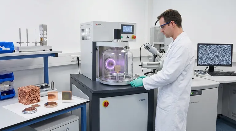
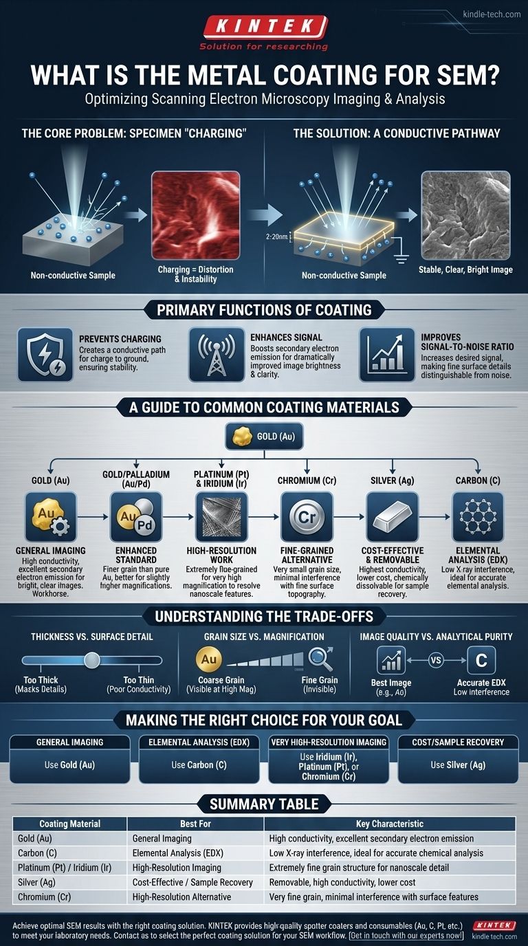
In Scanning Electron Microscopy (SEM), a metal coating is an ultra-thin layer of an electrically conductive material applied to a non-conductive sample. This process, known as sputter coating, typically uses materials like gold, platinum, silver, or carbon to prevent electrical charge build-up from the electron beam, which would otherwise severely distort the image.
The purpose of an SEM coating is to make a non-conductive sample visible to an electron microscope. The choice of material is a critical decision that balances the need for image clarity against the requirements of any subsequent chemical analysis.
Why a Coating is Necessary for SEM
Before selecting a material, it's essential to understand the fundamental problem that coating solves. SEM works by scanning a sample with a focused beam of electrons, and the resulting image is generated from the signals produced by this interaction.
The Core Problem: Specimen "Charging"
Non-conductive or poorly conductive specimens (like polymers, ceramics, or biological samples) cannot dissipate the electrical charge from the electron beam.
This charge accumulates on the surface, creating a static field that deflects the incoming electron beam. The result is a distorted, unstable, and often unusable image with bright patches and streaks.
The Solution: A Conductive Pathway
Sputter coating applies a very thin film of metal, typically between 2 and 20 nanometers, onto the sample.
This layer serves three primary functions:
- Prevents Charging: It creates a conductive path for the electrical charge to ground, ensuring a stable image.
- Enhances Signal: The metal coating is an excellent source of secondary electrons, the primary signal used for creating the SEM image, which dramatically improves image brightness and clarity.
- Improves Signal-to-Noise Ratio: By increasing the desired signal, the coating makes it easier to distinguish fine surface details from background noise.
A Guide to Common Coating Materials
The ideal coating material depends entirely on your analytical goal. Each metal offers a unique combination of conductivity, grain size, and chemical properties.
Gold (Au): The Workhorse for General Imaging
Gold is the most common coating material due to its high conductivity, chemical inertness, and ease of application. It provides excellent secondary electron emission, resulting in bright, clear images for a wide variety of applications.
Gold/Palladium (Au/Pd): An Enhanced Standard
An alloy of gold and palladium produces a finer grain structure than pure gold. This makes it a superior choice for imaging at slightly higher magnifications where the texture of the coating itself could become visible.
Platinum (Pt) & Iridium (Ir): For High-Resolution Work
These materials produce an extremely fine-grained coating. This is critical for very high-magnification imaging, as a coarser grain can obscure the nanoscale features you are trying to resolve on your sample's surface.
Chromium (Cr): A Fine-Grained Alternative
Chromium is another excellent choice for high-resolution applications. Its very small grain size ensures the coating itself does not interfere with observing the finest surface topography.
Silver (Ag): The Cost-Effective & Removable Option
Silver has the highest electrical conductivity of all metals and is a lower-cost alternative to gold. Its key advantage is that it can be chemically dissolved, allowing the original sample to be recovered for further study. However, it can tarnish over time.
Carbon (C): The Standard for Elemental Analysis
Carbon is the material of choice when performing Energy-Dispersive X-ray Spectroscopy (EDX). Metals like gold produce strong X-ray peaks that can overlap with and obscure the peaks of elements within the sample. Carbon's X-ray signal is very low and does not interfere, ensuring accurate elemental analysis.
Understanding the Trade-offs
Choosing a coating material is not just about picking the most conductive one. You must consider the inherent compromises.
Coating Thickness vs. Surface Detail
A coating must be thick enough to ensure conductivity but thin enough that it doesn't obscure the sample's surface features. A layer that is too thick will mask fine details, defeating the purpose of the analysis.
Grain Size vs. Magnification
At low magnification, the grain size of the coating material is irrelevant. However, at high magnification, the texture of a coarse-grained coating (like gold) can become visible, creating artifacts. Finer-grained materials (like iridium or chromium) are necessary to avoid this.
Image Quality vs. Analytical Purity
There is a direct trade-off between getting the best possible image and performing accurate chemical analysis. While gold produces a beautiful image, its signal will interfere with EDX. You must prioritize your primary goal.
Making the Right Choice for Your Goal
Base your selection on the information you need to extract from your sample.
- If your primary focus is general, routine imaging: Use Gold (Au) for its excellent performance and ease of use.
- If your primary focus is elemental analysis (EDX): You must use Carbon (C) to prevent X-ray signal interference.
- If your primary focus is very high-resolution imaging: Choose a fine-grained material like Iridium (Ir), Platinum (Pt), or Chromium (Cr).
- If your primary focus is cost or sample recovery: Use Silver (Ag), as it is less expensive and can be chemically removed after imaging.
Selecting the appropriate coating is the critical first step toward achieving clear, accurate, and meaningful SEM results.
Summary Table:
| Coating Material | Best For | Key Characteristic |
|---|---|---|
| Gold (Au) | General Imaging | High conductivity, excellent secondary electron emission |
| Carbon (C) | Elemental Analysis (EDX) | Low X-ray interference, ideal for accurate chemical analysis |
| Platinum (Pt) / Iridium (Ir) | High-Resolution Imaging | Extremely fine grain structure for nanoscale detail |
| Silver (Ag) | Cost-Effective / Sample Recovery | Removable, high conductivity, lower cost |
| Chromium (Cr) | High-Resolution Alternative | Very fine grain, minimal interference with surface features |
Achieve optimal SEM results with the right coating solution.
Choosing the correct coating material is essential for preventing charging, enhancing image clarity, and ensuring accurate analytical data. KINTEK specializes in providing high-quality sputter coaters and consumables—including gold, carbon, platinum, and other target materials—to meet your specific laboratory needs.
Whether you're focused on high-resolution imaging, elemental analysis, or sample recovery, our expertise ensures you get reliable, consistent performance. Contact us today to discuss your application and let our team help you select the perfect coating solution for your SEM workflow.
Get in touch with our experts now!
Visual Guide
Related Products
- Infrared Transmission Coating Sapphire Sheet Substrate Window
- Electrolytic Electrochemical Cell for Coating Evaluation
- Electron Beam Evaporation Coating Oxygen-Free Copper Crucible and Evaporation Boat
- Copper Foam
- Electrode Polishing Material for Electrochemical Experiments
People Also Ask
- What is organic thin film? A Guide to Engineered Molecular Layers for Advanced Tech
- What is the optical coating? Master Light Control for Superior Optical Performance
- What do optical coatings do? Control Light for Superior Optical Performance
- How can we create a reducing environment? Master the Methods for Precise Chemical Control
- Why do we need optical coating? To Control Light and Enhance Optical Performance