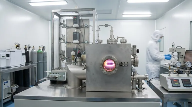
At its core, Plasma-Enhanced Chemical Vapor Deposition (PECVD) is a sophisticated process used to deposit very thin, high-performance films of material onto a substrate. This technique is critical in manufacturing advanced products, from the integrated circuits in your phone to the anti-scratch coatings on eyeglasses. It works by using an energized gas, or plasma, to drive the chemical reactions needed to create the film, which allows the process to run at much lower temperatures than conventional methods.
PECVD's defining advantage is its use of plasma to deposit high-quality films at low temperatures. This makes it indispensable for creating complex devices with sensitive underlying layers that would be damaged by the intense heat of traditional deposition techniques.
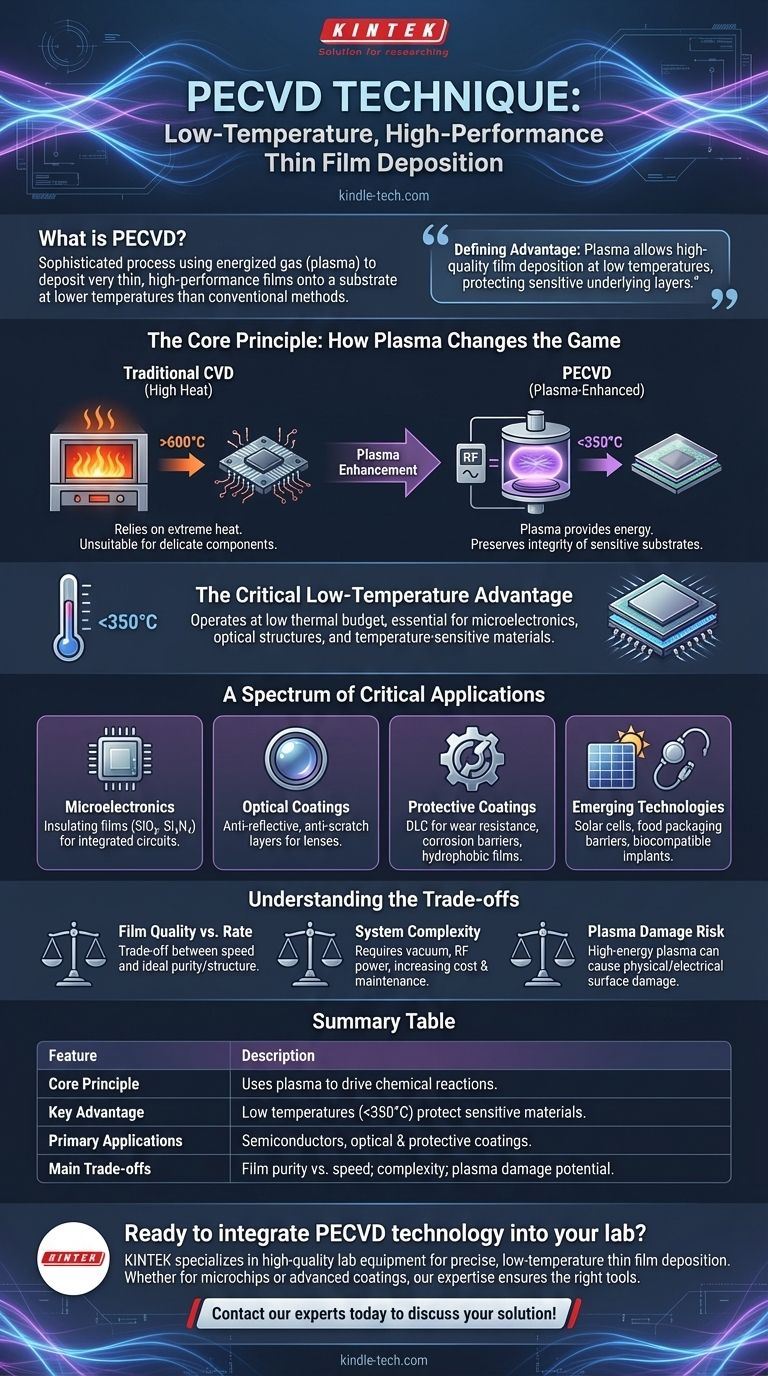
The Core Principle: How Plasma Changes the Game
To understand PECVD, it's helpful to first understand its predecessor, Chemical Vapor Deposition (CVD). The "plasma-enhanced" part is the key innovation that solves a fundamental manufacturing challenge.
The Limitation of Traditional CVD
Traditional Chemical Vapor Deposition relies on very high temperatures, often many hundreds of degrees Celsius. This heat provides the thermal energy needed for precursor gases to react and form a solid film on a substrate's surface.
This works well for robust, simple materials. However, it is completely unsuitable for building complex devices like a modern microprocessor, where delicate, previously fabricated circuits would be destroyed by such intense heat.
Introducing Plasma Enhancement
PECVD circumvents the need for extreme heat by introducing energy in a different form: plasma. Inside a vacuum chamber, an electric field is applied to the precursor gases, stripping electrons from their atoms and creating an ionized, highly reactive state of matter.
This plasma provides the energy required to break down the gas molecules and drive the chemical reactions. The film can then deposit and grow on the substrate surface without requiring high temperatures.
The Critical Low-Temperature Advantage
The ability to deposit high-quality films at temperatures often below 350°C is the primary reason PECVD is so widely used. This low thermal budget preserves the integrity of delicate microelectronic components, multi-layer optical structures, and other temperature-sensitive substrates.
A Spectrum of Critical Applications
The versatility and low-temperature nature of PECVD have made it a cornerstone technology across numerous high-tech industries. Its applications are defined by the need for precise, durable, and functional thin films.
Microelectronics and Semiconductors
This is the most common application. PECVD is essential for fabricating integrated circuits by depositing insulating (dielectric) films like silicon dioxide (SiO₂) and silicon nitride (Si₃N₄). These layers electrically isolate the millions of tiny conductive pathways on a chip, preventing short circuits.
Advanced Optical Coatings
PECVD is used to apply specialized coatings to lenses and other optical components. These films can create anti-reflective surfaces on camera lenses and sunglasses or highly durable anti-scratch layers that protect the underlying material.
Protective and Performance Coatings
The technology is used to create robust surface coatings on mechanical parts. These include ultra-hard Diamond-Like Carbon (DLC) films for wear resistance, corrosion-resistant barriers for industrial pipelines, and hydrophobic (water-repelling) films for various applications.
Emerging Technologies
PECVD is critical in the manufacturing of next-generation products. It is used to create layers within solar cells, apply protective barrier films for food packaging, and produce biocompatible coatings for medical implants that ensure they are accepted by the human body.
Understanding the Trade-offs
While powerful, PECVD is not a universal solution. Understanding its limitations is key to appreciating where it provides the most value.
Film Quality vs. Deposition Rate
The films produced by PECVD are generally high quality, but they can be less dense and contain more impurities (like hydrogen) than films grown at very high temperatures using other methods. There is often a trade-off between the speed of deposition and the ideal purity or structural integrity of the film.
System Complexity and Cost
A PECVD system is inherently more complex than a simple thermal CVD reactor. It requires a vacuum chamber, a gas delivery system, and a radio-frequency (RF) power source to generate the plasma. This complexity increases both the initial investment and ongoing maintenance costs.
Potential for Plasma-Induced Damage
While the low temperature of PECVD protects against thermal damage, the high-energy plasma itself can sometimes cause physical or electrical damage to the substrate surface. Engineers must carefully tune the plasma conditions to minimize this risk, especially when working with extremely sensitive electronic devices.
Making the Right Choice for Your Goal
Selecting a deposition technique depends entirely on the material constraints and performance requirements of the final product.
- If your primary focus is protecting sensitive electronic devices: PECVD is the industry standard for depositing high-quality insulating films without damaging underlying circuits.
- If your primary focus is creating high-performance surface coatings: PECVD offers a versatile method for producing hard, scratch-resistant, or water-repelling layers on a wide variety of materials.
- If your primary focus is fabricating advanced optical or photovoltaic devices: The precise control over film thickness and properties offered by PECVD is essential for managing light and energy.
Ultimately, PECVD is a foundational manufacturing process that enables the creation of the advanced materials that power modern technology.
Summary Table:
| Feature | Description |
|---|---|
| Core Principle | Uses plasma to drive chemical reactions for film deposition. |
| Key Advantage | Operates at low temperatures (<350°C), protecting sensitive materials. |
| Primary Applications | Semiconductor manufacturing, optical coatings, protective layers. |
| Main Trade-offs | Film purity vs. speed; system complexity and cost; potential plasma damage. |
Ready to integrate PECVD technology into your lab's workflow?
KINTEK specializes in providing high-quality lab equipment and consumables for all your deposition needs. Whether you are developing next-generation microchips, advanced optical coatings, or durable protective layers, our expertise ensures you have the right tools for precise, low-temperature thin film deposition.
Contact our experts today to discuss how our solutions can enhance your research and manufacturing processes!
Visual Guide
Related Products
- Chemical Vapor Deposition CVD Equipment System Chamber Slide PECVD Tube Furnace with Liquid Gasifier PECVD Machine
- RF PECVD System Radio Frequency Plasma-Enhanced Chemical Vapor Deposition RF PECVD
- Inclined Rotary Plasma Enhanced Chemical Vapor Deposition PECVD Equipment Tube Furnace Machine
- Inclined Rotary Plasma Enhanced Chemical Vapor Deposition PECVD Equipment Tube Furnace Machine
- 915MHz MPCVD Diamond Machine Microwave Plasma Chemical Vapor Deposition System Reactor
People Also Ask
- What is plasma enhanced chemical vapor deposition PECVD equipment? A Guide to Low-Temperature Thin Film Deposition
- What is the chemical vapor deposition growth process? Build Superior Thin Films from the Atom Up
- Why is Chemical Vapor Deposition (CVD) equipment uniquely suited for constructing hierarchical superhydrophobic structures?
- What are the core advantages of PE-CVD in OLED encapsulation? Protect Sensitive Layers with Low-Temp Film Deposition
- What are the advantages of chemical vapor deposition? Achieve Superior Thin Films for Your Lab


