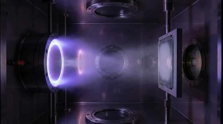
In essence, physical sputtering is a vacuum deposition technique where a solid material, known as a target, is bombarded with energetic ions from a plasma. This bombardment physically ejects atoms from the target surface through momentum transfer. These ejected atoms then travel through the vacuum chamber and deposit onto a substrate, gradually building up a highly controlled, uniform thin film.
Sputtering is not a chemical reaction but a physical momentum exchange process. It uses high-energy ions as atomic-scale "billiard balls" to knock atoms off a source material, which then recoat another surface with exceptional precision.
The Core Mechanism of Sputtering
To understand sputtering, it's best to visualize it as a sequence of distinct physical events occurring inside a controlled environment. Each step is critical for the formation of a high-quality thin film.
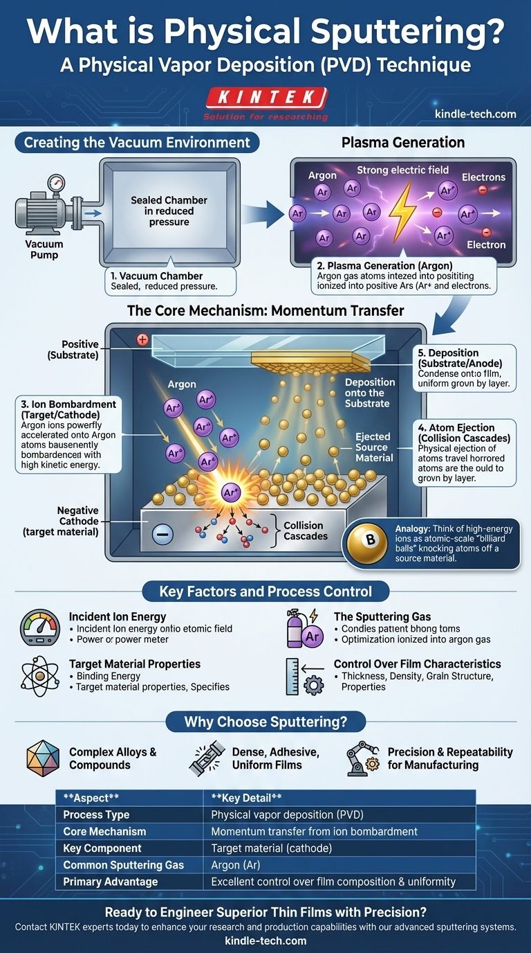
Creating the Vacuum Environment
The entire process must occur within a vacuum chamber. This removes atmospheric gases that could react with the sputtered atoms or interfere with their path to the substrate, ensuring the purity of the final film.
Generating the Plasma
A small amount of an inert gas, most commonly Argon (Ar), is introduced into the chamber. A strong electric field is then applied, with the source material (target) acting as the negative cathode and the substrate often acting as the positive anode. This field ionizes the argon atoms, stripping them of an electron and creating a mixture of positive argon ions and free electrons known as a plasma.
Bombarding the Target
The positively charged argon ions are powerfully accelerated by the electric field and crash into the negatively charged target surface. They strike the target with significant kinetic energy.
Ejecting Source Material
This high-energy ion bombardment sets off a series of "collision cascades" within the atomic structure of the target. Think of it as a subatomic chain reaction. When these cascades reach the surface, enough momentum is transferred to overcome the target's surface binding energy, physically ejecting atoms or molecules of the target material.
Deposition onto the Substrate
The ejected atoms travel in a vapor stream through the chamber. They eventually reach the substrate, where they condense and stick, forming a thin, uniform coating. The process is repeated billions of time per second, building the film one atomic layer at a time.
Key Factors and Process Control
The effectiveness and final result of the sputtering process are not accidental. They are governed by several key physical parameters that can be precisely controlled.
Incident Ion Energy
The energy of the bombarding ions is critical. If the energy is too low, no atoms will be ejected. If it's too high, the ions can become embedded in the target or cause damage. The optimal energy maximizes the sputter yield—the number of target atoms ejected per incident ion.
The Sputtering Gas
While Argon is common, other gases like Xenon can be used. The mass of the sputtering gas ions relative to the target atoms influences the efficiency of the momentum transfer, directly impacting the deposition rate.
Target Material Properties
The binding energy of the atoms in the target material plays a major role. Materials with lower binding energies are easier to sputter, meaning their atoms are dislodged with less force.
Control Over Film Characteristics
Because it is a physical, line-of-sight process, sputtering provides exceptional control over the final film. Engineers can precisely manage film thickness, density, grain structure, and electrical or optical properties by fine-tuning the gas pressure, voltage, and geometry within the chamber.
Making the Right Choice for Your Application
Sputtering is a highly versatile and powerful technique for creating high-performance coatings and electronic components. Understanding its strengths helps determine if it's the right choice for a specific goal.
- If your primary focus is depositing complex alloys or compounds: Sputtering excels at preserving the original material's composition in the final film, which is difficult with heat-based evaporation methods.
- If your primary focus is creating dense, adhesive, and uniform films: The high kinetic energy of sputtered atoms results in coatings with superior density and adhesion compared to many other techniques.
- If your primary focus is precision and repeatability for manufacturing: Sputtering offers fine control over film thickness and properties, making it ideal for processes requiring high consistency, like in semiconductor or optical filter production.
This method stands as a cornerstone of modern materials science, enabling the creation of advanced materials with precisely engineered properties.
Summary Table:
| Aspect | Key Detail |
|---|---|
| Process Type | Physical vapor deposition (PVD) |
| Core Mechanism | Momentum transfer from ion bombardment |
| Key Component | Target material (cathode) |
| Common Sputtering Gas | Argon (Ar) |
| Primary Advantage | Excellent control over film composition and uniformity |
Ready to Engineer Superior Thin Films with Precision?
At KINTEK, we specialize in providing advanced lab equipment, including sputtering systems, to meet the exacting demands of materials science and manufacturing. Whether you are developing semiconductor components, optical coatings, or specialized alloys, our solutions deliver the repeatability and control you need for high-performance results.
Contact our experts today to discuss how our sputtering technology can enhance your research and production capabilities.
Visual Guide
Related Products
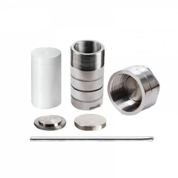
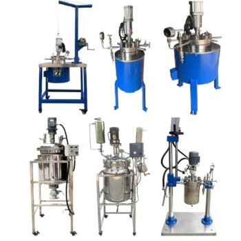
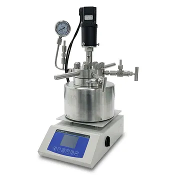
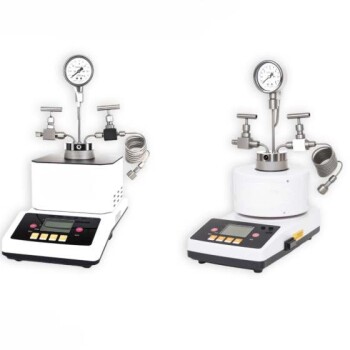
- High Pressure Laboratory Autoclave Reactor for Hydrothermal Synthesis
- Stainless High Pressure Autoclave Reactor Laboratory Pressure Reactor
- Mini SS High Pressure Autoclave Reactor for Laboratory Use
- Customizable High Pressure Reactors for Advanced Scientific and Industrial Applications
- Customizable Laboratory High Temperature High Pressure Reactors for Diverse Scientific Applications
People Also Ask
- How does a hydrothermal reactor facilitate growth on carbon nanofibers? Optimize Your Material Synthesis
- Why is a 24-hour hydrothermal treatment in an autoclave necessary for BMO nanosheets? Unlock Superior Photocatalysis
- What role does a high-pressure reactor (autoclave) play in the synthesis of NiCuFe-LDH? Master Hydrothermal Growth
- What function do high-pressure autoclaves serve in the hydrothermal synthesis? Master High-Crystallinity Catalyst Design
- What Role Does a High-Pressure Reactor or Autoclave Play in HA Catalyst Synthesis? Achieve High Surface Area Materials