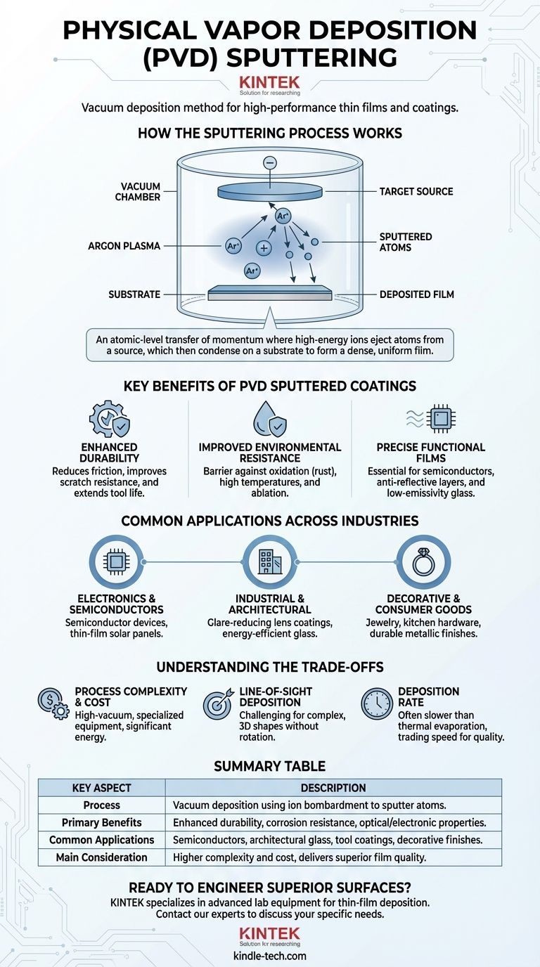
At its core, Physical Vapor Deposition (PVD) Sputtering is a vacuum deposition method used to create high-performance thin films and coatings. The process works by bombarding a solid source material, known as the "target," with high-energy ions, which ejects or "sputters" atoms from the source. These vaporized atoms then travel through the vacuum and deposit onto a substrate, forming a thin, highly uniform film.
The central purpose of PVD Sputtering is not merely to coat an object, but to fundamentally alter its surface properties. It is a precise, atom-by-atom construction process that imparts new mechanical, optical, or electronic functions to a material.
How the Sputtering Process Works
Sputtering is a highly controlled process that takes place inside a vacuum chamber. This environment is critical for ensuring the purity and quality of the final film.
The Atomic "Billiard Shot"
The mechanism is best understood as an atomic-level transfer of momentum. An inert gas, typically Argon, is introduced into the chamber and ionized, creating a plasma.
An electric field accelerates these positive Argon ions, causing them to collide with the negatively charged target material with tremendous force. This bombardment dislodges individual atoms from the target surface.
Deposition and Film Growth
These sputtered atoms travel through the vacuum and condense on the surface of the object being coated (the substrate).
Because this happens atom by atom, the resulting film is extremely thin, dense, and uniform, perfectly mirroring the surface of the substrate it covers.
Key Benefits of PVD Sputtered Coatings
The value of PVD sputtering lies in the functional improvements it provides to a substrate's surface. The process is chosen for its ability to deliver superior performance characteristics.
Enhanced Durability and Hardness
Sputtered coatings create an incredibly hard surface layer. This is used to reduce friction, improve scratch resistance, and significantly extend the life of tools and components.
Improved Environmental Resistance
These films act as a powerful barrier against environmental factors. They are used to improve oxidation resistance (preventing rust and corrosion) and protect parts from high temperatures and ablation, which is critical in aerospace applications.
Precise Functional Films
PVD allows for the creation of films with specific optical or electronic properties. This is essential for manufacturing semiconductor circuits, anti-reflective layers on eyeglasses, and low-emissivity coatings on architectural glass that improve thermal efficiency.
Common Applications Across Industries
PVD sputtering is a versatile technology applied to both high-tech components and everyday consumer products, demonstrating its wide range of capabilities.
Electronics and Semiconductor Fabrication
The process is fundamental to modern electronics. It is used to deposit the thin conductive and insulating layers required for semiconductor devices, thin-film transistors, and thin-film solar panels.
Industrial and Architectural Uses
In large-scale manufacturing, sputtering is used to apply specialized coatings to glass. These include coatings that reduce glare on optical lenses and those that block infrared radiation on architectural glass, making buildings more energy-efficient.
Decorative and Consumer Goods
PVD provides a durable and brilliant finish for consumer products. It is widely used on jewelry, kitchen and bathroom hardware, and other decorative items to create a finish that is far more resilient than traditional plating and does not require polishing to achieve a metallic luster.
Understanding the Trade-offs
While powerful, PVD sputtering is a sophisticated process with specific operational considerations that make it ideal for some applications but less suited for others.
Process Complexity and Cost
Sputtering requires a high-vacuum environment, specialized equipment, and significant energy input. This makes it a more complex and costly process compared to simple painting or electroplating.
Line-of-Sight Deposition
The sputtered material travels in a relatively straight line from the target to the substrate. This can make it challenging to achieve a perfectly uniform coating on highly complex, three-dimensional shapes without advanced substrate rotation systems.
Deposition Rate
Compared to other PVD methods like thermal evaporation, sputtering can have a lower deposition rate. The trade-off is often speed for the exceptional density, adhesion, and uniformity of the sputtered film.
Making the Right Choice for Your Goal
Selecting PVD sputtering depends entirely on the desired outcome for the final product's surface.
- If your primary focus is extreme durability: Sputtering is the ideal choice for creating hard, wear-resistant, and corrosion-proof surfaces for industrial tools, medical implants, and aerospace components.
- If your primary focus is precision electronic or optical function: This process provides the atomic-level control needed to create the ultra-thin, pure, and uniform layers required for semiconductors, sensors, and specialized glass.
- If your primary focus is a premium, long-lasting aesthetic finish: PVD sputtering delivers a brilliant, tarnish-resistant metallic coating for luxury goods and high-end hardware that far surpasses traditional finishing methods.
Ultimately, PVD sputtering empowers engineers and designers to engineer the surface of a material, fundamentally enhancing its value and performance.
Summary Table:
| Key Aspect | Description |
|---|---|
| Process | Vacuum deposition method using ion bombardment to sputter atoms from a target onto a substrate. |
| Primary Benefits | Enhanced durability, corrosion resistance, precise optical/electronic properties, and decorative finishes. |
| Common Applications | Semiconductor fabrication, architectural glass coatings, durable tool coatings, and high-end decorative finishes. |
| Main Consideration | Higher complexity and cost than traditional plating, but delivers superior film quality and performance. |
Ready to engineer superior surfaces with PVD sputtering?
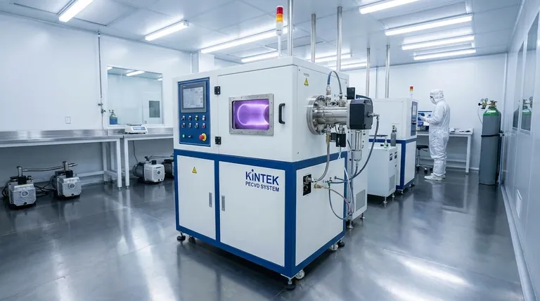
KINTEK specializes in advanced lab equipment and consumables for precise thin-film deposition. Whether you are developing semiconductors, durable tool coatings, or innovative optical products, our solutions help you achieve the high-performance, uniform films your research and production demand.
Contact our experts today to discuss how we can support your specific laboratory needs and coating challenges.
Visual Guide
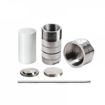
Related Products
- RF PECVD System Radio Frequency Plasma-Enhanced Chemical Vapor Deposition RF PECVD
- Inclined Rotary Plasma Enhanced Chemical Vapor Deposition PECVD Equipment Tube Furnace Machine
- Evaporation Boat for Organic Matter
- Chemical Vapor Deposition CVD Equipment System Chamber Slide PECVD Tube Furnace with Liquid Gasifier PECVD Machine
- Microwave Plasma Chemical Vapor Deposition MPCVD Machine System Reactor for Lab and Diamond Growth
People Also Ask
- What are the advantages of PECVD? Enable Low-Temperature, High-Quality Thin-Film Deposition
- What is plasma activated chemical vapour deposition method? A Low-Temperature Solution for Advanced Coatings
- Why is PECVD environment friendly? Understanding the Eco-Friendly Benefits of Plasma-Enhanced Coating
- What are the applications of PECVD? Essential for Semiconductors, MEMS, and Solar Cells
- How does RF power create plasma? Achieve Stable, High-Density Plasma for Your Applications