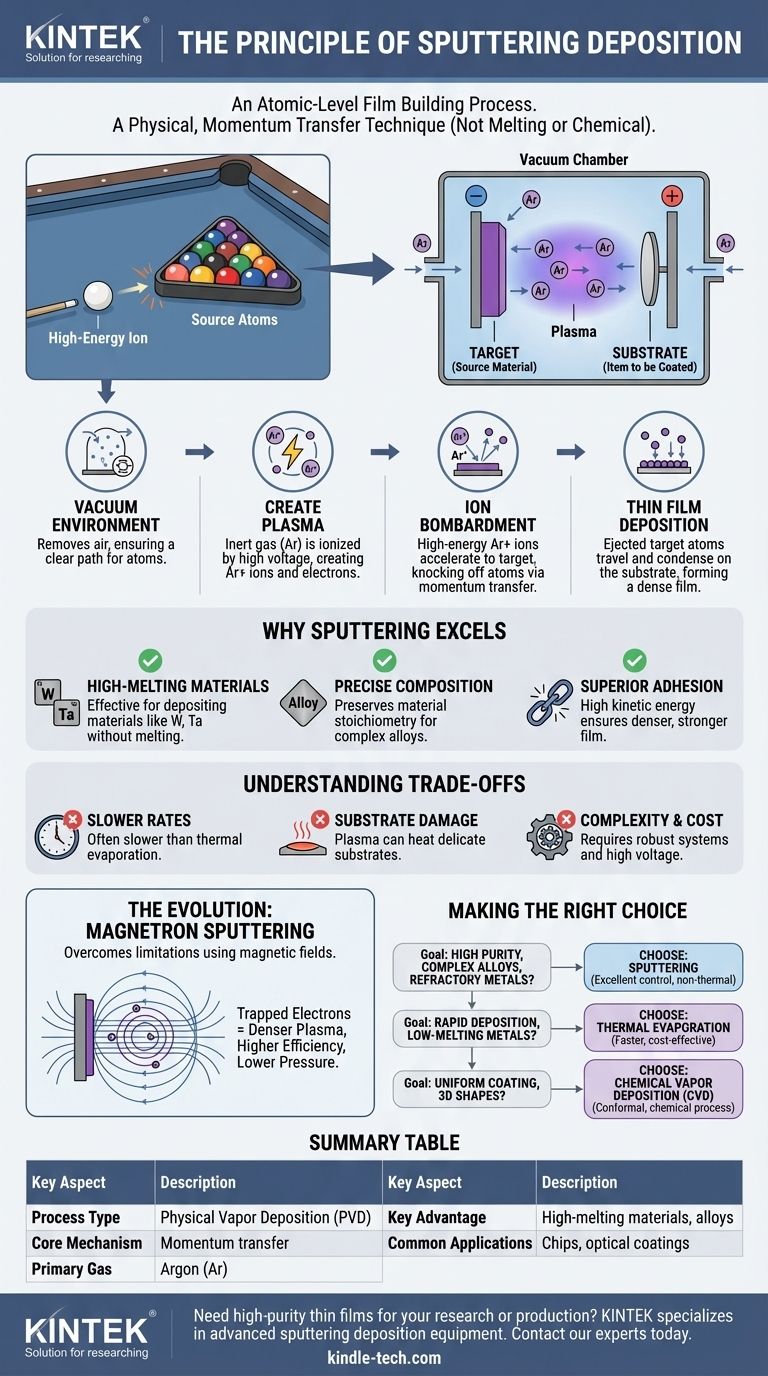
At its core, sputtering deposition is a physical process where high-energy ions are used to dislodge atoms from a source material, similar to how a cue ball scatters racked billiard balls. These dislodged atoms then travel through a vacuum and deposit onto a substrate, building a new layer one atom at a time. This technique is a cornerstone of modern manufacturing, used to create the ultra-thin, high-performance films found in everything from semiconductor chips to anti-reflective coatings on eyeglasses.
Sputtering is not a melting or chemical process; it is a momentum transfer technique. It uses the kinetic energy of charged gas ions to physically knock atoms off a target, allowing for the precise deposition of materials—especially those with very high melting points or complex compositions—that are difficult to handle with other methods.
The Core Mechanism: From Plasma to Film
Sputtering is a type of Physical Vapor Deposition (PVD) that relies on a sequence of precise physical events occurring within a controlled vacuum chamber.
The Vacuum Environment: A Clear Path
The entire process happens in a vacuum chamber pumped down to a very low pressure.
This vacuum is critical because it removes air and other particles, ensuring the sputtered atoms can travel from the target to the substrate without colliding with unwanted contaminants.
Creating the Plasma: Igniting the Gas
An inert gas, most commonly argon (Ar), is introduced into the chamber. A high voltage is then applied between two electrodes: a negatively charged cathode (which holds the source material, or target) and a positively charged anode (which holds the item to be coated, or substrate).
This strong electric field energizes free electrons, causing them to collide with argon atoms and knock off an electron. This creates positively charged argon ions (Ar+) and more free electrons, resulting in a self-sustaining, glowing plasma.
The Bombardment: Ejecting Target Atoms
The newly formed, positively charged argon ions (Ar+) are powerfully accelerated toward the negatively charged target.
Upon impact, these high-energy ions transfer their momentum to the atoms of the target material, knocking them loose. This ejection of target atoms is the "sputtering" event.
The Deposition: Forming the Thin Film
The ejected target atoms travel through the vacuum and land on the surface of the substrate.
As these atoms accumulate, they condense and form a thin, solid, and often highly dense film. The properties of this film can be precisely controlled by adjusting parameters like gas pressure, voltage, and temperature.
Why Sputtering Excels: Key Advantages
Sputtering is not always the fastest or cheapest deposition method, but it is chosen when quality, precision, and material versatility are paramount.
Handling Difficult Materials
Because sputtering does not rely on melting or evaporating the source material, it is exceptionally effective for depositing materials with extremely high melting points, like tungsten or tantalum.
Precise Control Over Film Composition
Sputtering is ideal for depositing alloys and compound materials. The process physically transfers atoms from the target to the substrate, generally preserving the original material's stoichiometry (the proportional ratio of elements).
Superior Adhesion and Density
Sputtered atoms arrive at the substrate with significantly more kinetic energy than atoms from a simple evaporation process. This energy helps them form a denser, stronger, and more adherent film on the substrate surface.
Understanding the Trade-offs
No technique is perfect. Understanding the limitations of sputtering is key to using it effectively.
Slower Deposition Rates
In its basic form, sputtering is often slower than other methods like thermal evaporation. While modern advancements have improved speeds, it can be a bottleneck in high-volume production.
Potential for Substrate Damage
The energetic plasma and ion bombardment can heat the substrate. For delicate substrates like plastics or certain biological samples, this unintentional heating can cause damage or deformation.
System Complexity and Cost
Sputtering systems are mechanically complex. They require robust vacuum pumps, high-voltage power supplies, and precise gas flow controllers, making them more expensive to purchase and maintain than simpler deposition setups.
The Evolution: Magnetron Sputtering
To overcome the limitations of basic sputtering, nearly all modern systems use a technique called magnetron sputtering.
The Problem with Basic Sputtering
In a simple system, electrons are quickly lost to the anode, making the plasma inefficient. This requires operating at higher gas pressures, which unfortunately leads to more scattering of the sputtered atoms and lower-quality films.
The Magnetic Field Solution
Magnetron sputtering places a powerful magnetic field directly behind the target material.
This magnetic field traps electrons near the surface of the target, forcing them into a long, spiral path. This dramatically increases the probability that an electron will collide with and ionize an argon atom, creating a much denser and more stable plasma.
The Result: Faster, Better, and More Controllable
This enhanced ionization efficiency allows the system to operate at much lower pressures. This results in higher deposition rates, less scattering, and ultimately, higher-purity films with better properties.
Making the Right Choice for Your Goal
The decision to use sputtering depends entirely on your material requirements and production goals.
- If your primary focus is high-purity films of complex alloys or refractory metals: Sputtering is the superior choice due to its non-thermal nature and excellent compositional control.
- If your primary focus is rapid deposition of simple, low-melting-point metals: Thermal evaporation may be a more cost-effective and faster alternative.
- If your primary focus is a uniform, conformal coating over complex 3D shapes: Chemical Vapor Deposition (CVD) is often a better fit, as it is a chemical process and not limited by line-of-sight deposition.
Ultimately, sputtering provides an unparalleled level of control for engineering high-performance surfaces at the atomic scale.
Summary Table:
| Key Aspect | Description |
|---|---|
| Process Type | Physical Vapor Deposition (PVD) |
| Core Mechanism | Momentum transfer from high-energy ions to target atoms |
| Primary Gas Used | Argon (Ar) |
| Key Advantage | Excellent for high-melting-point materials and complex alloys |
| Common Applications | Semiconductor chips, anti-reflective coatings, precision optics |
Need high-purity thin films for your research or production? KINTEK specializes in advanced sputtering deposition equipment and consumables for laboratory and industrial applications. Our solutions deliver superior film adhesion, precise compositional control, and exceptional material versatility—perfect for handling complex alloys and refractory metals. Contact our experts today to discuss how our sputtering systems can enhance your coating process and achieve your specific material engineering goals.
Visual Guide
Related Products
- Chemical Vapor Deposition CVD Equipment System Chamber Slide PECVD Tube Furnace with Liquid Gasifier PECVD Machine
- RF PECVD System Radio Frequency Plasma-Enhanced Chemical Vapor Deposition RF PECVD
- Customer Made Versatile CVD Tube Furnace Chemical Vapor Deposition Chamber System Equipment
- Custom CVD Diamond Coating for Lab Applications
- HFCVD Machine System Equipment for Drawing Die Nano-Diamond Coating
People Also Ask
- What are the core advantages of PE-CVD in OLED encapsulation? Protect Sensitive Layers with Low-Temp Film Deposition
- What is the chemical vapor deposition growth process? Build Superior Thin Films from the Atom Up
- What are the advantages of chemical vapor deposition? Achieve Superior Thin Films for Your Lab
- How are carbon nanotubes grown? Master Scalable Production with Chemical Vapor Deposition
- How expensive is chemical vapor deposition? Understanding the True Cost of High-Performance Coating


