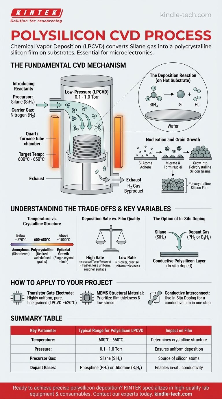
In essence, polysilicon is created through Chemical Vapor Deposition (CVD) by introducing a silicon-containing gas, most commonly silane (SiH₄), into a high-temperature reaction chamber. The heat causes the gas to decompose, depositing a solid film of polycrystalline silicon onto a substrate, such as a silicon wafer. This process is fundamental to manufacturing integrated circuits and other microelectronic devices.
The core principle of polysilicon CVD is not just about depositing silicon, but about precisely controlling temperature and pressure. These variables are the levers that determine the film's final crystalline structure, which in turn dictates its electrical and mechanical properties for a specific application.
The Fundamental CVD Mechanism for Polysilicon
Chemical Vapor Deposition is a group of processes, but for creating polysilicon, the industry overwhelmingly relies on a specific type known as Low-Pressure CVD (LPCVD). This method allows for uniform deposition across many wafers at once.
Introducing the Reactants
The process begins by introducing a precise mixture of gases into a vacuum chamber.
The primary reactant, or precursor, is silane gas (SiH₄). This gas contains the silicon atoms that will form the final film. Inert carrier gases, like nitrogen (N₂), are often used to control the concentration and flow of the silane.
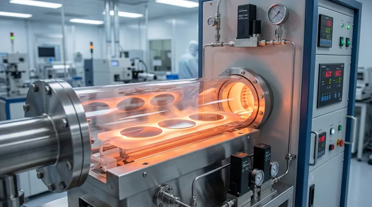
The Reaction Chamber and Substrate
Substrates, typically silicon wafers that may already have a layer of silicon dioxide (SiO₂), are loaded into a quartz furnace tube. In an LPCVD system, these wafers are often stacked vertically in a "boat" to maximize the number of wafers processed in a single run.
Once the chamber is sealed and pumped down to a low pressure (typically 0.1 to 1.0 Torr), it is heated to the target reaction temperature.
The Role of Temperature and Pressure
Temperature is the most critical variable in the entire process. For the deposition of polysilicon, the furnace is maintained in a narrow range, typically between 600°C and 650°C.
This specific temperature provides enough thermal energy to break the chemical bonds in the silane gas molecules when they reach the hot wafer surface.
The Deposition Reaction
On the hot substrate surface, the silane thermally decomposes according to the following chemical reaction:
SiH₄ (gas) → Si (solid) + 2H₂ (gas)
The solid silicon (Si) atoms adhere to the substrate surface, while the hydrogen gas (H₂) byproduct is continuously pumped out of the reaction chamber.
Nucleation and Grain Growth
The deposited silicon atoms do not form a random, disordered layer. Instead, they migrate on the hot surface and arrange themselves into small, ordered crystal structures called nuclei.
As more silicon atoms deposit, these nuclei grow into larger grains. The final film is a composite of these tightly packed, randomly oriented grains, which gives the material its name: polycrystalline silicon.
Understanding the Trade-offs and Key Variables
Achieving a high-quality polysilicon film requires a careful balancing act. The process parameters you choose directly impact the film's characteristics and manufacturing efficiency.
Temperature vs. Crystalline Structure
The deposition temperature directly determines the silicon's structure. This relationship is fundamental to materials engineering in semiconductor fabrication.
- Below ~570°C: The atoms lack sufficient energy to form ordered crystals, resulting in an amorphous silicon film.
- ~600-650°C: This is the ideal range for forming a polycrystalline structure with well-defined grains.
- Above ~1000°C: The process shifts toward epitaxial growth, where the deposited film mimics the single-crystal structure of the underlying silicon substrate (a different process for different goals).
Deposition Rate vs. Film Quality
Manufacturers are always trying to balance speed with quality. Increasing the temperature or the silane gas pressure will increase the deposition rate, allowing more wafers to be processed per hour.
However, a very high deposition rate can lead to a rougher surface and less uniform film thickness. For applications requiring extreme precision, a slower, more controlled deposition rate at the lower end of the temperature range is often preferred.
The Option of In-Situ Doping
Polysilicon in its pure form is a poor conductor. To be useful as a gate electrode or interconnect, it must be "doped" with impurities like phosphorus or boron to make it conductive.
This can be done after deposition, but it can also be performed in-situ (during the process) by adding a small amount of a dopant gas like phosphine (PH₃) or diborane (B₂H₆) to the silane gas stream. This creates a doped, conductive polysilicon layer in a single step.
How to Apply This to Your Project
The ideal process parameters are dictated entirely by the end-use of the polysilicon film.
- If your primary focus is creating a transistor gate electrode: You need a highly uniform, pure, and fine-grained film, making LPCVD near 620°C the standard. Doping is often performed later via ion implantation for precise control.
- If your primary focus is a structural material in MEMS: You may prioritize film thickness and low stress over electrical properties, allowing for slightly different temperature and pressure regimes.
- If your primary focus is creating a conductive interconnect: You will likely use in-situ doping with phosphine or diborane during deposition to save a process step and create a conductive film from the start.
Ultimately, mastering polysilicon CVD is a matter of balancing reaction kinetics with the desired electronic and structural properties of the final film.
Summary Table:
| Key Parameter | Typical Range for Polysilicon LPCVD | Impact on Film |
|---|---|---|
| Temperature | 600°C - 650°C | Determines crystalline structure (amorphous, poly, or epitaxial) |
| Pressure | 0.1 - 1.0 Torr | Ensures uniform deposition across wafers |
| Precursor Gas | Silane (SiH₄) | Source of silicon atoms for the film |
| Dopant Gases | Phosphine (PH₃) or Diborane (B₂H₆) | Enables in-situ conductivity for interconnects |
Ready to achieve precise polysilicon deposition for your microelectronics or MEMS project? KINTEK specializes in high-quality lab equipment and consumables for semiconductor fabrication. Our expertise ensures you get the uniform, controlled films critical for integrated circuits and sensors. Contact our experts today to discuss how we can support your CVD process needs.
Visual Guide
Related Products
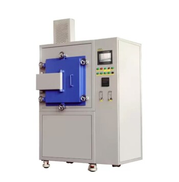
- Multi Heating Zones CVD Tube Furnace Machine Chemical Vapor Deposition Chamber System Equipment
- Customer Made Versatile CVD Tube Furnace Chemical Vapor Deposition Chamber System Equipment
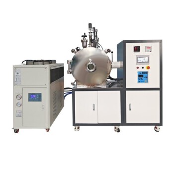
- Chemical Vapor Deposition CVD Equipment System Chamber Slide PECVD Tube Furnace with Liquid Gasifier PECVD Machine
- Horizontal High Temperature Graphite Vacuum Graphitization Furnace
- Inclined Rotary Plasma Enhanced Chemical Vapor Deposition PECVD Equipment Tube Furnace Machine
People Also Ask
- What is the substrate for CVD process? Choosing the Right Foundation for Your Thin Film
- What are the advantages of a multi-zone tube furnace for Sb2S3? Unlock Superior Semiconductor Thin Film Purity
- What is the difference between hot wall CVD and cold wall CVD? Choose the Right System for Your Process
- What are the differences between chemical vapour deposition processes? A Guide to Pressure, Quality & Cost
- How does a CVD tube furnace inhibit the sintering of silver supports? Boost Membrane Durability and Performance