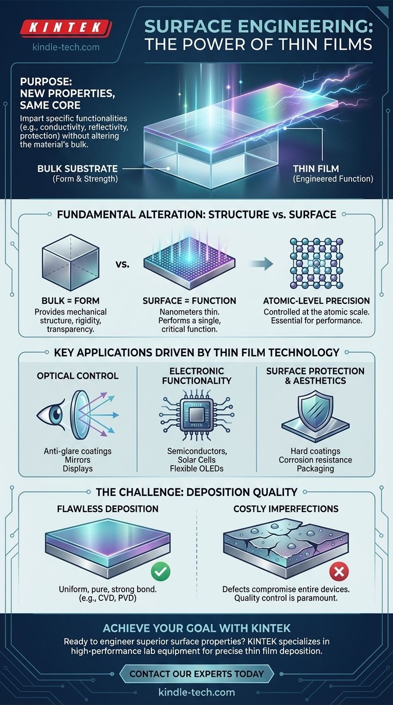
The fundamental purpose of creating a thin film is to impart entirely new properties to a material's surface without altering the bulk characteristics of the material itself. This technique allows us to add specific functionalities—like electrical conductivity, optical reflectivity, or corrosion resistance—to a standard substrate such as glass, silicon, or metal. A common mirror, for instance, is simply a sheet of glass with a thin metallic film on the back to make it reflective.
At its core, thin film technology is about surface engineering. It enables us to take an ordinary, inexpensive material and give its surface extraordinary, high-performance capabilities tailored to a specific function.
How Thin Films Fundamentally Alter a Material
The power of this technology lies in separating a material's structural role from its surface function. The base material provides the form and strength, while the incredibly thin layer applied to it provides a highly specialized and engineered property.
From Bulk Properties to Surface Functionality
A substrate, such as a silicon wafer or a piece of architectural glass, provides the necessary physical structure. It is chosen for its mechanical strength, rigidity, or transparency.
The thin film, often just nanometers to micrometers thick, is then deposited onto this substrate. This layer is engineered to perform a single, critical function, such as conducting electricity, filtering light, or resisting scratches.
The Importance of Atomic-Level Precision
In many modern applications, especially semiconductors, the precision of these films is paramount. As electronic components like computer chips continue to shrink, the quality of their constituent thin films becomes the primary factor limiting performance.
The deposition of these layers must be controlled at the atomic or molecular scale. Even a few misplaced atoms or a slight impurity in the film can create a defect that compromises the function of the entire device.
Key Applications Driven by Thin Film Technology
The ability to precisely modify surfaces enables a vast range of modern technologies. We can group these applications by the primary function the thin film provides.
Manipulating Light with Optical Coatings
Thin films are essential for controlling how light reflects, transmits, or is absorbed. A single layer or multiple layers can be stacked to create highly specific optical properties.
Applications include anti-reflection coatings on ophthalmic lenses, mirrored surfaces on lamps, thermal insulation coatings on architectural glass, and the transparent conductive films used in touch-panel displays.
Controlling Electricity in Modern Electronics
The entire semiconductor industry is built upon the precise deposition of thin films. These films create the transistors, conductors, and insulators that form integrated circuits.
This category also includes thin-film photovoltaic cells for solar energy, the polymer compounds used in flexible OLED screens, and even the components of thin-film batteries.
Enhancing Durability and Aesthetics
Many thin films serve a protective or decorative purpose. They create a durable barrier between the core material and the environment.
Examples include hard, wear-resistant coatings on cutting tools, thin layers of chromium on bathroom fittings to prevent corrosion while adding shine, and protective polymer films on food packaging to preserve freshness.
Understanding the Primary Challenge: Deposition Quality
The value of a thin film is entirely dependent on the quality of its application. The process of depositing the film is just as critical as the material being used, as imperfections can lead to total failure.
The Critical Role of Deposition Methods
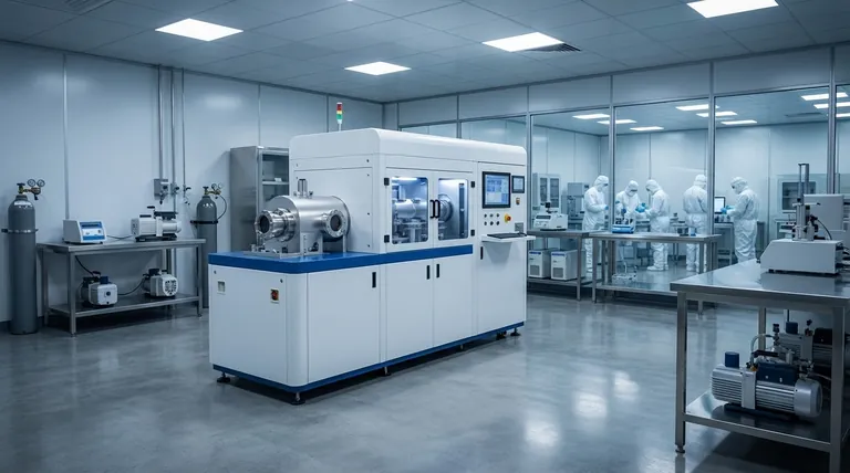
Techniques like Chemical Vapour Deposition (CVD) and Physical Vapour Deposition (PVD) are used to apply films with atomic-level accuracy.
The goal of any deposition method is to create a film that is perfectly uniform, pure, and strongly bonded to the substrate. The manufacturing conditions must be meticulously controlled to achieve this.
Why Imperfections Are So Costly
In a complex device like a microchip, which contains dozens of thin film layers, a single defect can ruin the entire component.
A microscopic crack, an area of poor adhesion, or a chemical impurity can disrupt electrical flow or alter optical properties, rendering the final product useless. This makes quality control the central challenge in high-performance thin film applications.
Making the Right Choice for Your Goal
Applying thin film technology effectively requires a clear understanding of the desired outcome. The ideal film and deposition process are dictated by the specific surface property you need to engineer.
- If your primary focus is optical performance: Your goal is precise control over film thickness and refractive index to manipulate light, as seen in anti-glare lenses.
- If your primary focus is electronic functionality: The purity and atomic-level uniformity of the film are paramount to ensure reliable performance in devices like microchips.
- If your primary focus is surface protection: The key is creating a dense, non-porous barrier that adheres strongly to the substrate to prevent corrosion or physical wear.
Ultimately, mastering surface properties through thin films is a cornerstone of modern material science and technological advancement.
Summary Table:
| Purpose | Key Function | Common Applications |
|---|---|---|
| Optical Control | Manipulate light reflection, transmission, or absorption | Anti-glare coatings, mirrors, display screens |
| Electronic Functionality | Enable conductivity, insulation, or semiconductor properties | Microchips, solar cells, flexible OLEDs |
| Surface Protection & Aesthetics | Enhance durability, corrosion resistance, or appearance | Hard coatings on tools, chrome plating, packaging films |
Ready to engineer superior surface properties for your materials?
At KINTEK, we specialize in high-performance lab equipment and consumables for precise thin film deposition. Whether you're developing optical coatings, electronic components, or protective layers, our solutions ensure atomic-level precision and reliability.
Let us help you achieve flawless thin films that meet your specific application goals. Contact our experts today to discuss your project needs!
Visual Guide
Related Products
- Tungsten Evaporation Boat for Thin Film Deposition
- Aluminum-Plastic Flexible Packaging Film for Lithium Battery Packaging
- Thin-Layer Spectral Electrolysis Electrochemical Cell
- Lab Plastic PVC Calender Stretch Film Casting Machine for Film Testing
People Also Ask
- What is the difference between PVD and CVD? Choose the Right Thin-Film Deposition Technique
- What is a thin film evaporator? A Gentle Solution for Heat-Sensitive & Viscous Materials
- What is the process of thin film deposition? A Guide to PVD, CVD, and Coating Techniques
- What methods are used to deposit thin films? A Guide to PVD, CVD, and ALD Techniques
- What are the types of thin film? A Guide to PVD vs. CVD Deposition Methods


