In essence, reactive sputtering is a thin-film deposition technique where a reactive gas, like oxygen or nitrogen, is intentionally introduced into a vacuum chamber during the standard sputtering process. This gas chemically reacts with the atoms ejected from a pure material target, forming a new compound material that then deposits as a thin film onto a substrate.
The critical distinction is that reactive sputtering isn't just about physically moving a material from a source to a substrate; it's a process of synthesizing a new compound material directly onto a surface, allowing for precise control over its chemical composition and properties.
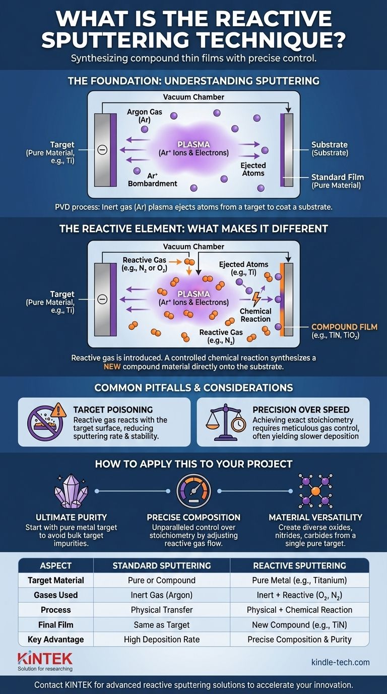
The Foundation: Understanding Sputtering
The Core Sputtering Process
Sputtering is a type of Physical Vapor Deposition (PVD). The process begins with a target, which is the source material you want to deposit, and a substrate, which is the surface you want to coat.
Both are placed in a vacuum chamber that is backfilled with an inert gas, almost always argon.
Creating a Plasma
A strong negative voltage is applied to the target. This electrical field energizes the argon gas, stripping electrons from the atoms and creating a plasma—a glowing state of matter consisting of positive argon ions and free electrons.
Bombardment and Deposition
These positively charged argon ions are accelerated with great force toward the negatively charged target. The high-energy impact physically knocks atoms loose from the target material.
These ejected atoms travel through the vacuum chamber and land on the substrate, gradually building up a thin film layer by layer.
The Reactive Element: What Makes It Different
Introducing the Reactive Gas
Reactive sputtering builds directly upon this foundation. The key difference is the introduction of a second, reactive gas (such as oxygen or nitrogen) into the chamber along with the inert argon gas.
A Controlled Chemical Reaction
As atoms are ejected from the pure metal target, they travel through the plasma and interact with the reactive gas. This triggers a chemical reaction in-flight or on the substrate surface itself.
For example, if you sputter a titanium (Ti) target while introducing nitrogen (N₂) gas, the titanium atoms will react with the nitrogen to form titanium nitride (TiN).
Forming a Compound Film
The material that ultimately deposits onto the substrate is this newly synthesized compound. This method allows for the creation of very specific compound films, such as oxides, nitrides, or carbides, starting from a pure, often metallic, target.
Common Pitfalls and Considerations
The Challenge of Process Control
The most significant challenge in reactive sputtering is managing the chemical reaction. The process is highly sensitive to the flow rates of the inert and reactive gases.
If too much reactive gas is introduced, it can begin to react with the surface of the target itself, a phenomenon known as "target poisoning." This can drastically reduce the sputtering rate and create instability in the process.
Precision Over Speed
Achieving the desired stoichiometry—the exact chemical ratio of elements in the compound film—requires meticulous control over gas pressures and power levels.
While this precision is the primary advantage of the technique, it often means the deposition rates are slower compared to sputtering directly from a pre-made compound target.
How to Apply This to Your Project
The decision to use reactive sputtering is driven by the specific properties required for the final thin film.
- If your primary focus is ultimate purity: Use reactive sputtering, as starting with a pure metal target avoids the impurities often present in bulk compound targets.
- If your primary focus is precise chemical composition: This technique offers unparalleled control over stoichiometry by simply adjusting the reactive gas flow.
- If your primary focus is material versatility: Reactive sputtering is highly efficient, allowing you to create many different types of compound films (e.g., oxides, nitrides) from a single pure target just by changing the reactive gas.
Reactive sputtering transforms a simple physical deposition process into a powerful tool for material synthesis, enabling the engineering of advanced films with tailored properties.
Summary Table:
| Aspect | Standard Sputtering | Reactive Sputtering |
|---|---|---|
| Target Material | Pure or Compound | Pure Metal (e.g., Titanium) |
| Gases Used | Inert Gas (Argon) | Inert Gas (Argon) + Reactive Gas (O₂, N₂) |
| Process | Physical Transfer | Physical Transfer + Chemical Reaction |
| Final Film | Same as Target | New Compound (e.g., TiO₂, TiN) |
| Key Advantage | High Deposition Rate | Precise Control over Film Composition & Purity |
Ready to engineer thin films with precise composition and superior purity for your research or production?
At KINTEK, we specialize in advanced lab equipment, including sputtering systems designed for reliable reactive processes. Whether you need to deposit oxides, nitrides, or other compound films, our expertise can help you achieve the exact material properties your project demands.
Contact our experts today to discuss how a KINTEK reactive sputtering solution can accelerate your innovation.
Visual Guide
Related Products
- Spark Plasma Sintering Furnace SPS Furnace
- Chemical Vapor Deposition CVD Equipment System Chamber Slide PECVD Tube Furnace with Liquid Gasifier PECVD Machine
- RF PECVD System Radio Frequency Plasma-Enhanced Chemical Vapor Deposition RF PECVD
- Customer Made Versatile CVD Tube Furnace Chemical Vapor Deposition Chamber System Equipment
- Vacuum Induction Melting Spinning System Arc Melting Furnace
People Also Ask
- What is the pressure for spark plasma sintering? A Guide to Optimizing SPS Parameters
- What are the advantages of CAMI/SPS for W-Cu composite preparation? Reduce cycles from hours to seconds.
- What are the fundamentals of spark plasma sintering process? Unlock Rapid, High-Performance Material Consolidation
- What is the difference between spark plasma sintering and flash sintering? A Guide to Advanced Sintering Methods
- What is SPS sintering method? A Guide to High-Speed, High-Performance Material Fabrication


