Sputtering is a highly controlled deposition process used to create exceptionally thin and uniform films. In a vacuum, a solid source material, known as the "target," is bombarded with high-energy ions from a gas plasma. This bombardment physically knocks atoms off the target, which then travel and deposit onto a component, called the "substrate," forming a precise coating.
Sputtering is fundamentally a process of momentum transfer, not evaporation. It uses the physical impact of ions to eject atoms from a source material, allowing for precise control over the resulting film's structure, density, and composition on a microscopic level.
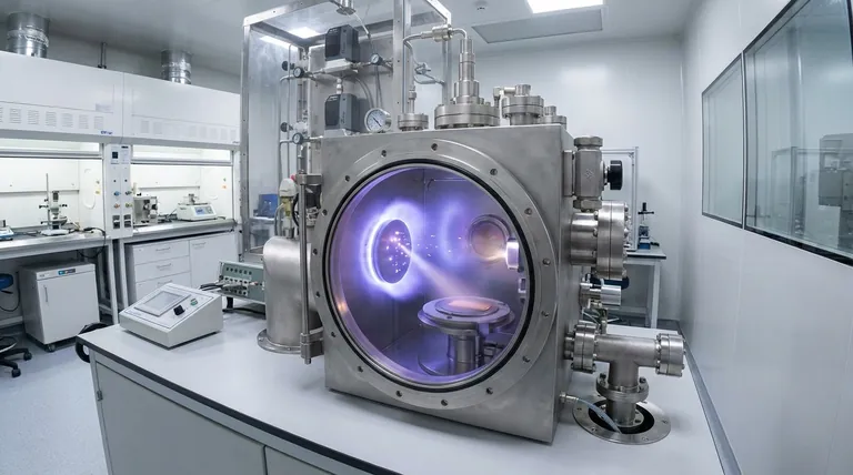
The Core Mechanism: From Plasma to Film
Sputtering is a physical vapor deposition (PVD) method that occurs in a series of well-defined steps inside a vacuum chamber.
Setting the Stage: The Vacuum Chamber
The process begins by placing the target (the source material for the film) and the substrate (the part to be coated) into a vacuum chamber. The chamber is evacuated to remove air and other contaminants that could interfere with the process.
Igniting the Plasma: The Role of Inert Gas
A small amount of an inert gas, most commonly Argon, is introduced into the chamber. A high voltage is applied, creating a negative charge on the target (making it the cathode) and a positive charge on the substrate or chamber walls (the anode).
This voltage energizes the gas, stripping electrons from the Argon atoms and creating a plasma—a glowing, ionized gas consisting of positive Argon ions and free electrons.
The Bombardment: Momentum Transfer in Action
The positively charged Argon ions are forcefully accelerated toward the negatively charged target. They strike the target's surface with significant kinetic energy.
This impact initiates collision cascades within the target's atomic structure. The energy is transferred from the ion to the target atoms, and if an atom near the surface receives enough momentum to overcome its atomic binding energy, it is ejected or "sputtered" from the target.
The Deposition: Coating the Substrate
The ejected atoms travel in a straight line through the vacuum chamber until they strike the substrate. Upon arrival, these atoms condense on the surface, nucleate, and grow into a thin, uniform film.
For precise control, a shutter is often placed between the target and substrate. This allows the sputtering process to stabilize before the shutter is opened to begin deposition.
Understanding the Trade-offs
While powerful, sputtering is not a universal solution. Understanding its limitations is key to using it effectively.
Lower Deposition Rates
Compared to thermal evaporation, sputtering can be a slower process. The rate of material transfer is limited by the efficiency of the ion bombardment, which can extend process times for thicker films.
Process Complexity and Heat
Sputtering systems are more complex and expensive than simple thermal evaporators. The constant ion bombardment also generates significant heat in the target, which often requires active cooling systems to prevent damage or changes in material properties.
Potential for Gas Incorporation
There is a small chance that ions from the sputtering gas (e.g., Argon) can become embedded in the growing film. This can alter the film's properties, such as its electrical resistivity or internal stress, which must be accounted for in sensitive applications.
Making the Right Choice for Your Goal
Selecting sputtering depends entirely on the required properties of the final film.
- If your primary focus is a dense, uniform film with high adhesion: Sputtering is an excellent choice, as the energetic atoms embed slightly into the substrate, creating a strong bond.
- If you need to deposit materials with high melting points or complex alloys: Sputtering is superior to thermal evaporation because it can deposit virtually any material without needing to melt it.
- If your primary focus is coating a simple material as quickly as possible: You might evaluate thermal evaporation, which can offer higher deposition rates for certain materials at a lower equipment cost.
By understanding sputtering as a physical process of controlled atomic transfer, you can leverage its precision to engineer films with highly specific characteristics.
Summary Table:
| Aspect | Description |
|---|---|
| Process Type | Physical Vapor Deposition (PVD) |
| Core Mechanism | Momentum transfer from ion bombardment |
| Key Advantage | Dense, uniform films with excellent adhesion |
| Ideal For | Materials with high melting points, alloys, complex compositions |
| Common Gas Used | Argon |
Need a precise, high-quality coating for your application? KINTEK specializes in advanced lab equipment, including sputtering systems, to help you achieve superior thin films with excellent uniformity and adhesion. Our experts are ready to assist you in selecting the right solution for your laboratory's specific materials and research goals. Contact our team today to discuss your project!
Visual Guide

Related Products
- Chemical Vapor Deposition CVD Equipment System Chamber Slide PECVD Tube Furnace with Liquid Gasifier PECVD Machine
- Customer Made Versatile CVD Tube Furnace Chemical Vapor Deposition Chamber System Equipment
- RF PECVD System Radio Frequency Plasma-Enhanced Chemical Vapor Deposition RF PECVD
- Custom CVD Diamond Coating for Lab Applications
- Aluminized Ceramic Evaporation Boat for Thin Film Deposition
People Also Ask
- What are the core advantages of PE-CVD in OLED encapsulation? Protect Sensitive Layers with Low-Temp Film Deposition
- What is the chemical vapor deposition growth process? Build Superior Thin Films from the Atom Up
- What are the advantages of chemical vapor deposition? Achieve Superior Thin Films for Your Lab
- How expensive is chemical vapor deposition? Understanding the True Cost of High-Performance Coating
- How are carbon nanotubes grown? Master Scalable Production with Chemical Vapor Deposition


