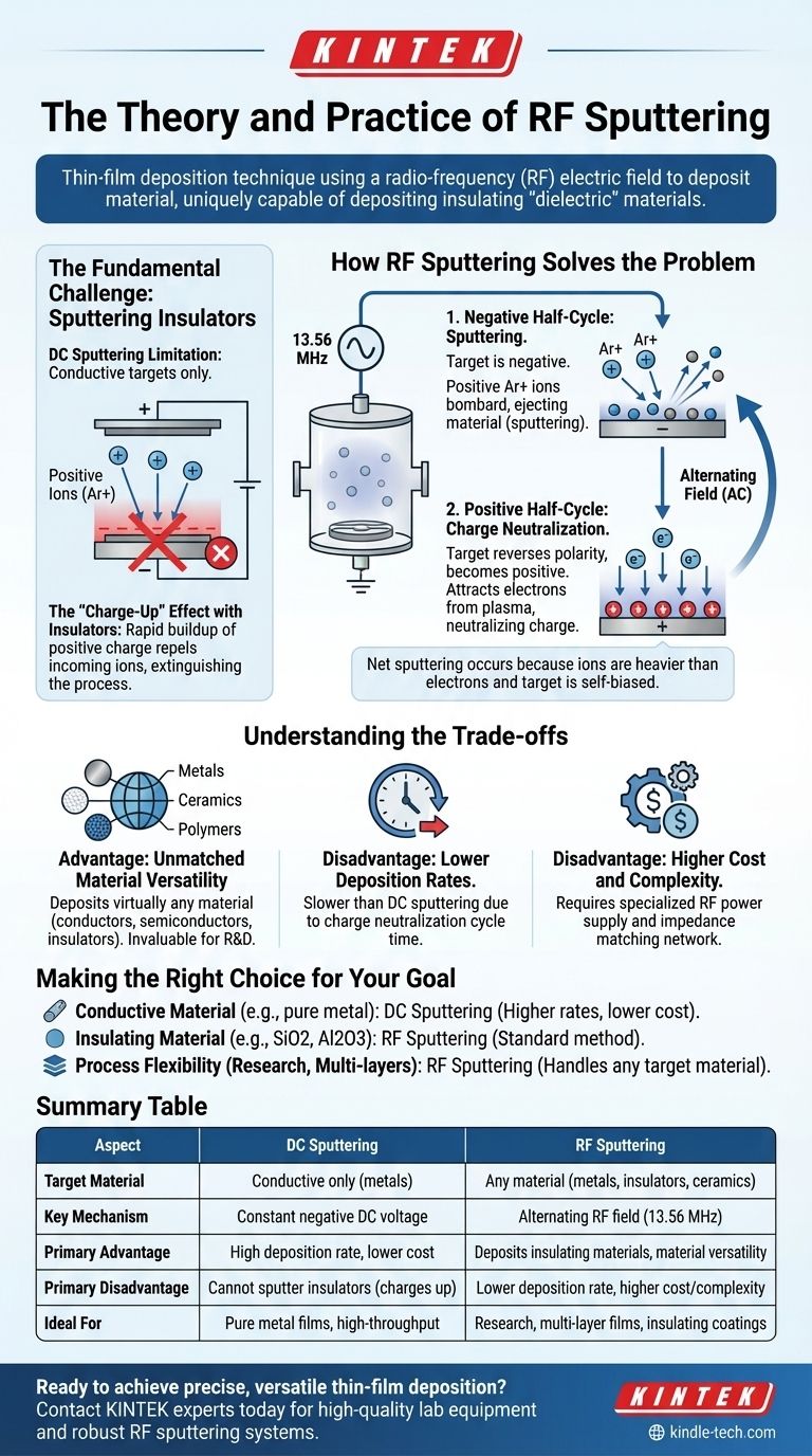
At its core, RF sputtering is a thin-film deposition technique that uses a radio-frequency (RF) electric field to create a plasma and deposit material onto a surface. Unlike its simpler counterpart, DC sputtering, this method is uniquely capable of depositing insulating or "dielectric" materials, making it a cornerstone of modern materials science and semiconductor manufacturing.
The fundamental purpose of RF sputtering is to overcome the primary limitation of DC sputtering: the inability to deposit non-conductive materials. It achieves this by using an alternating current to periodically neutralize electrical charge that builds up on the surface of an insulating target, allowing the sputtering process to be sustained.
The Fundamental Challenge: Sputtering Insulators
To understand the value of RF sputtering, you must first understand the problem it was designed to solve. This problem lies within the physics of its predecessor, DC sputtering.
The DC Sputtering Limitation
In a standard DC (Direct Current) sputtering system, the target material must be electrically conductive. The target is held at a large negative DC voltage, and the chamber walls or a discrete anode are grounded. This creates a circuit, allowing a continuous flow of current.
Positive ions (typically argon, Ar+) from the plasma are accelerated toward the negative target. They strike the target with high energy, dislodging or "sputtering" atoms of the target material. This works perfectly for metals.
The "Charge-Up" Effect with Insulators
If you attempt to sputter an insulating material (like a ceramic or oxide) with a DC source, the process fails almost immediately.
As positive Ar+ ions bombard the insulating target surface, their positive charge cannot be conducted away. This results in a rapid buildup of positive charge on the target face, a phenomenon known as "charging".
This positive surface layer effectively repels the incoming positive Ar+ ions from the plasma, neutralizing the electric field and extinguishing the sputtering process entirely.
How RF Sputtering Solves the Problem
RF sputtering ingeniously solves the charging problem by replacing the static DC voltage with a high-frequency AC (Alternating Current) voltage.
The Alternating Field
The system uses an AC power source operating in the radio-frequency range, almost universally fixed at the industry-standard 13.56 MHz. This frequency is high enough to sustain a plasma efficiently but has a critical effect on the target surface.
The Negative Half-Cycle: Sputtering
During the first half of the AC cycle, the target becomes negatively charged relative to the plasma. Just as in DC sputtering, this large negative potential attracts the positive Ar+ ions.
These ions bombard the target, initiating collision cascades that eject atoms of the target material. This is the primary deposition part of the cycle.
The Positive Half-Cycle: Charge Neutralization
During the second half of the cycle, the target's polarity reverses, and it becomes positively charged. At this moment, the target attracts the most mobile charged particles in the plasma: electrons.
A brief but intense flow of electrons floods the target surface, neutralizing the positive charge that was built up by ion bombardment during the previous half-cycle. This effectively "resets" the surface, preventing the fatal charge-up effect.
Because the target is self-biased to have a larger negative voltage period than a positive one, and because ions are much heavier than electrons, net sputtering of the target material still occurs.
Understanding the Trade-offs
Choosing RF sputtering involves a clear set of trade-offs against other deposition methods. Your application's requirements will determine if these trade-offs are acceptable.
Advantage: Unmatched Material Versatility
The single greatest advantage of RF sputtering is its ability to deposit virtually any material. This includes all metals, alloys, semiconductors, ceramics, polymers, and other insulating compounds. This flexibility makes it an invaluable research and development tool.
Disadvantage: Lower Deposition Rates
RF sputtering is generally slower than DC sputtering. Part of each AC cycle is dedicated to charge neutralization rather than material ejection. This "off time" for sputtering means it takes longer to grow a film of the same thickness compared to a DC process running on a conductive target.
Disadvantage: Higher Cost and Complexity
RF systems are inherently more complex. They require a specialized RF power supply and an impedance matching network—a critical component that ensures maximum power is transferred from the supply to the plasma. This additional hardware increases the cost and technical complexity of the equipment.
Making the Right Choice for Your Goal
Your decision to use RF sputtering should be based on the type of material you need to deposit and your priorities for speed and cost.
- If your primary focus is depositing a conductive material (like a pure metal): DC sputtering is often the superior choice, offering higher deposition rates and lower equipment cost.
- If your primary focus is depositing an insulating material (like silicon dioxide or aluminum oxide): RF sputtering is the standard and necessary method to prevent target charging.
- If your primary focus is process flexibility for research or complex multi-layers: RF sputtering provides the versatility to handle any target material, making it an ideal choice for labs that work with a wide range of materials.
By understanding the interplay between the target material and the applied electric field, you can confidently select the deposition technique that aligns perfectly with your engineering goals.
Summary Table:
| Aspect | DC Sputtering | RF Sputtering |
|---|---|---|
| Target Material | Conductive only (metals) | Any material (metals, insulators, ceramics) |
| Key Mechanism | Constant negative DC voltage | Alternating RF field (13.56 MHz) |
| Primary Advantage | High deposition rate, lower cost | Deposits insulating materials, material versatility |
| Primary Disadvantage | Cannot sputter insulators (charges up) | Lower deposition rate, higher cost/complexity |
| Ideal For | Pure metal films, high-throughput production | Research, multi-layer films, insulating coatings |
Ready to achieve precise, versatile thin-film deposition in your lab?
Whether you are developing advanced semiconductor devices, creating specialized optical coatings, or researching novel materials, the right sputtering system is critical to your success. KINTEK specializes in providing high-quality lab equipment, including robust RF sputtering systems designed for reliability and performance.
We understand the challenges of working with insulating materials and complex multi-layer structures. Our expertise can help you select the ideal equipment to enhance your research and development capabilities.
Contact our experts today to discuss your specific application needs and discover how KINTEK's solutions can drive your innovations forward.
Visual Guide
Related Products
- RF PECVD System Radio Frequency Plasma-Enhanced Chemical Vapor Deposition RF PECVD
- Horizontal High Temperature Graphite Vacuum Graphitization Furnace
- Spark Plasma Sintering Furnace SPS Furnace
- Automatic Laboratory Hydraulic Press for XRF & KBR Pellet Press
- Electron Beam Evaporation Coating Oxygen-Free Copper Crucible and Evaporation Boat
People Also Ask
- What is the role of RF-PECVD in VFG preparation? Mastering Vertical Growth and Surface Functionality
- What is plasma chemical vapor deposition? A Low-Temperature Thin Film Coating Solution
- Why is a Matching Network Indispensable in RF-PECVD for Siloxane Films? Ensure Stable Plasma and Uniform Deposition
- What is plasma enhanced chemical Vapour deposition process used for fabrication of? A Guide to Low-Temperature Thin Films
- What is plasma enhanced chemical vapour deposition process? Unlock Low-Temperature, High-Quality Thin Films


