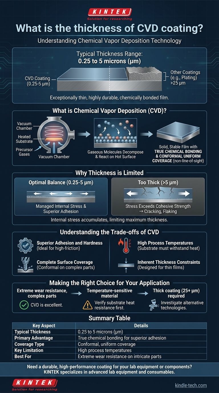
In most industrial applications, the thickness of a Chemical Vapor Deposition (CVD) coating typically ranges from 0.25 to 5 microns (µm). This process creates an exceptionally thin yet highly durable and wear-resistant film. The coating is not merely applied to the surface; it is chemically bonded to the substrate at a molecular level.
The core principle to understand is that CVD creates an ultra-thin, high-performance film by "growing" it directly onto a part through a chemical reaction. This process results in superior adhesion but also introduces internal stresses that inherently limit the coating's maximum thickness.
What is Chemical Vapor Deposition (CVD)?
CVD is a sophisticated coating process that transforms gaseous molecules into a solid material directly on the surface of a substrate. It's less like painting and more like precisely controlling a chemical reaction to build a new surface layer atom by atom.
The Core Process Explained
The process involves placing a part, or substrate, inside a reactor chamber under vacuum. Volatile precursor gases are then introduced. When the chamber is heated to a specific reaction temperature, these gases decompose and react on the hot substrate, forming a solid, stable film that bonds to the surface.
True Chemical Bonding
Unlike many other coating methods, CVD creates a true chemical bond between the coating and the substrate material. For example, to create a Titanium Nitride (TiN) coating, gases like Titanium Tetrachloride (TiCl₄) and Nitrogen (N₂) are used, reacting to form a new, integrated layer. This results in exceptional adhesion that is difficult to replicate with other methods.
Conformal, Uniform Coverage
A key advantage of CVD is its non-line-of-sight nature. Because the coating is formed from a gas that fills the entire chamber, it can deposit a uniform film on all exposed surfaces of a part. This includes complex geometries, blind holes, threads, and internal passages that are impossible to coat with line-of-sight processes like PVD.
Why Thickness is Limited
The thickness of a CVD coating is not arbitrary; it's a direct consequence of the deposition process itself. The key factors are the balance of deposition speed and the management of internal stress.
The Balance of Deposition and Stress
As the coating film is built up layer by layer, internal stress accumulates within the material. If the coating becomes too thick, this stress can exceed the material's cohesive strength, leading to cracking, flaking, or delamination from the substrate. The 0.25 to 5-micron range represents the optimal balance between performance and structural integrity.
Process Control and Repeatability
The final thickness is precisely managed by controlling variables like temperature, gas flow rates, pressure, and deposition time. Modern CVD processes offer excellent repeatability, ensuring consistent coating thickness from one batch to the next.
Understanding the Trade-offs of CVD
Like any advanced process, CVD has a distinct set of advantages and limitations that make it suitable for specific applications.
Advantage: Superior Adhesion and Hardness
The chemical bond created during the CVD process results in unparalleled adhesion. The resulting coatings are often extremely hard and highly resistant to abrasion and wear, making them ideal for cutting tools and high-friction components.
Advantage: Complete Surface Coverage
For parts with intricate or irregular shapes, like drill bits or end mills, CVD's ability to provide a conformal coating is a critical advantage. It ensures every functional surface receives protection.
Limitation: High Process Temperatures
CVD is an elevated temperature process. This heat is necessary to drive the chemical reaction but limits the types of base materials that can be coated. The substrate must be able to withstand the process temperature without warping, melting, or losing its essential properties.
Limitation: Inherent Thickness Constraints
The process is fundamentally designed for creating thin films. Applications requiring a very thick buildup of material (well beyond 5 microns) are not a good fit for CVD due to the internal stress limitations.
Making the Right Choice for Your Application
Choosing the right coating technology depends entirely on your project's specific requirements.
- If your primary focus is extreme wear resistance on complex parts: CVD is an excellent choice due to its conformal nature and the superior adhesion of its chemically-bonded, hard coatings.
- If your primary focus is coating a temperature-sensitive material: You must first verify that the substrate can withstand the high temperatures of the CVD process without being compromised.
- If your primary focus requires a thick coating (e.g., 25+ microns): You should investigate alternative technologies like thermal spray or plating, as CVD is fundamentally a thin-film process.
Ultimately, understanding that CVD's strength lies in its thin, chemically-bonded nature is the key to leveraging its unique advantages for the right applications.
Summary Table:
| Key Aspect | Details |
|---|---|
| Typical Thickness Range | 0.25 to 5 microns (µm) |
| Primary Advantage | True chemical bonding for superior adhesion |
| Coverage Type | Conformal, uniform coverage on complex geometries |
| Key Limitation | High process temperatures (substrate must withstand heat) |
| Best For | Extreme wear resistance on intricate parts |
Need a durable, high-performance coating for your lab equipment or components?
The precise, ultra-thin films created by Chemical Vapor Deposition (CVD) offer unparalleled wear resistance and uniform coverage, even on complex parts. KINTEK specializes in providing advanced lab equipment and consumables, including coating solutions tailored to laboratory needs.
We can help you determine if CVD is the right choice for your application, ensuring optimal performance and longevity.
Contact our experts today via our Contact Form to discuss your specific requirements and discover the benefits we can bring to your laboratory.
Visual Guide
Related Products
- Custom CVD Diamond Coating for Lab Applications
- HFCVD Machine System Equipment for Drawing Die Nano-Diamond Coating
- CVD Diamond Dressing Tools for Precision Applications
- Battery Lab Equipment 304 Stainless Steel Strip Foil 20um Thick for Battery Test
- CVD Diamond for Thermal Management Applications
People Also Ask
- What is CVD coating used for? Hardening Tools & Building Semiconductors for Industry
- How thick is CVD diamond coating? Balancing Durability and Stress for Optimal Performance
- What is the use of CVD coating? Enhance Durability and Functionality for Your Components
- What are the different CVD coating? A Guide to Thermal CVD, PECVD, and Specialized Methods
- Can you coat something in diamond? Unlock Unmatched Hardness and Thermal Conductivity


