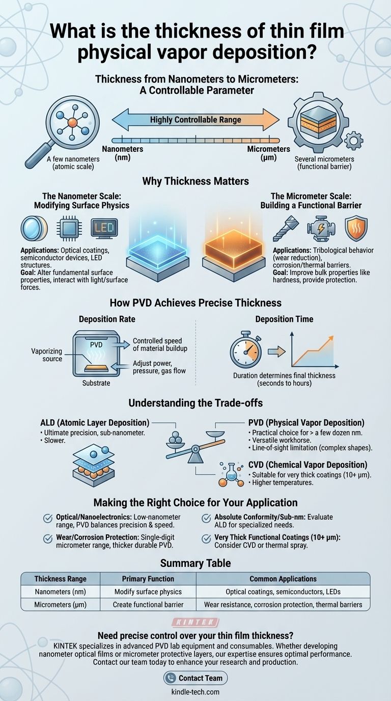
In practice, a thin film created by Physical Vapor Deposition (PVD) can range in thickness from a few nanometers (just a handful of atoms) up to several micrometers. While the broader category of thin films can technically extend to 100 micrometers, most PVD applications operate well below this, focusing on the nanometer-to-micron scale to impart specific surface properties without changing the bulk material.
The thickness of a PVD coating is not a fixed number but a highly controllable parameter. The critical insight is that this precise control—from atomic-scale layers to durable functional coatings—is what makes PVD a cornerstone technology for enhancing modern materials and devices.
Why Thickness Is the Defining Parameter
The specific thickness of a PVD coating is intentionally chosen because it directly dictates the film's function. A few nanometers can have a dramatically different effect than a few micrometers of the same material.
The Nanometer Scale: Modifying Surface Physics
At the nanometer scale, films are so thin that they primarily interact with light and surface forces. The goal here is not to add bulk but to alter the fundamental properties of the substrate's surface.
Applications in this range include optical coatings on lenses to control reflection and transmission, creating the layers in semiconductor devices, and forming the light-emitting structures in LED displays. The film is often thinner than a wavelength of light.
The Micrometer Scale: Building a Functional Barrier
As thickness increases into the micrometer range (1 µm = 1,000 nm), the coating begins to act as a distinct physical layer. Its own bulk properties, such as hardness and chemical resistance, become dominant.
These thicker films are used to improve tribological behavior (reducing friction and wear on tools or engine parts) and provide robust corrosion or thermal barriers. The coating serves as a protective shield for the underlying material.
How PVD Achieves Precise Thickness
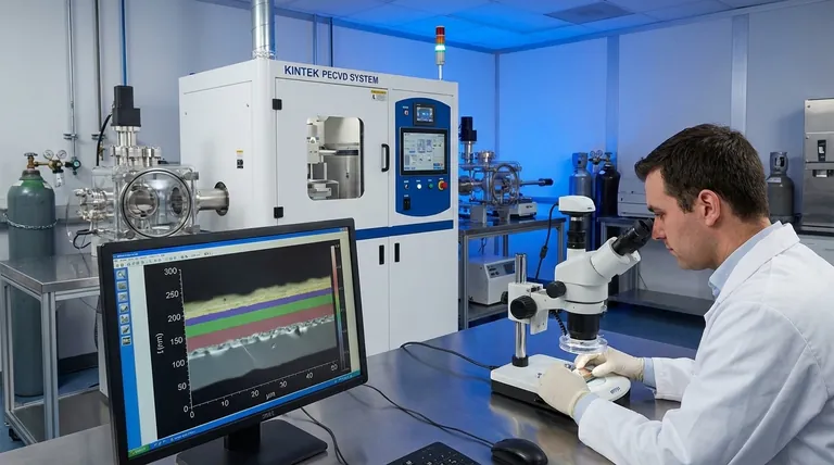
PVD is not a single process but a family of techniques, including sputtering and evaporation. In all cases, a source material is vaporized in a vacuum and condenses onto a substrate, giving engineers multiple levers to control the final film thickness.
Deposition Rate
The primary factor is the deposition rate, which is the speed at which the coating material builds up on the substrate surface. This rate is controlled by adjusting process parameters like power, pressure, and gas flow inside the PVD chamber.
Deposition Time
The most straightforward control is deposition time. Once a stable deposition rate is established, the final thickness is simply a function of how long the substrate is exposed to the vapor source. This allows for highly repeatable results, from seconds for nanometer-thin films to hours for thick, wear-resistant coatings.
Understanding the Trade-offs
PVD is a versatile workhorse, but its capabilities are best understood in context with other deposition methods. The required thickness is often a deciding factor in which technology is chosen.
PVD vs. Atomic Layer Deposition (ALD)
ALD is a process that deposits a film literally one atomic layer at a time. It offers the ultimate in precision, conformity, and thickness control at the sub-nanometer level. However, this precision comes at the cost of speed; ALD is significantly slower than PVD. PVD is the more practical choice for films thicker than a few dozen nanometers.
PVD vs. Chemical Vapor Deposition (CVD)
CVD uses chemical reactions on the substrate surface to grow a film. It can often achieve higher deposition rates than PVD, making it suitable for very thick coatings (tens to hundreds of microns). However, CVD typically requires much higher substrate temperatures, which can damage sensitive materials like plastics or certain electronics.
The Line-of-Sight Limitation
A key characteristic of PVD is that it is a line-of-sight process. The vaporized material travels in a straight line from the source to the substrate. While excellent for coating flat surfaces, this can make it difficult to uniformly coat complex, three-dimensional shapes without sophisticated part rotation.
Making the Right Choice for Your Application
The ideal film thickness is entirely dependent on your end goal. The versatility of PVD allows it to serve many different needs, but you must match the thickness to the desired function.
- If your primary focus is optical performance or nanoelectronics: You will be operating in the low-nanometer range where PVD provides a good balance of precision and speed.
- If your primary focus is wear resistance or corrosion protection: You will need a thicker, more durable coating in the single-digit micrometer range.
- If your primary focus is absolute conformity and sub-nanometer precision: You should evaluate Atomic Layer Deposition (ALD) as a more specialized alternative.
- If your primary focus is creating very thick functional coatings (10+ µm): You may find that Chemical Vapor Deposition (CVD) or thermal spray processes are more economical.
Ultimately, controlling film thickness is how PVD engineering transforms an ordinary material into a high-performance component.
Summary Table:
| Thickness Range | Primary Function | Common Applications |
|---|---|---|
| Nanometers (nm) | Modify surface physics | Optical coatings, semiconductors, LEDs |
| Micrometers (µm) | Create functional barrier | Wear resistance, corrosion protection, thermal barriers |
Need precise control over your thin film thickness? KINTEK specializes in advanced PVD lab equipment and consumables, helping you achieve the exact coating specifications your application demands. Whether you're developing nanometer-scale optical films or durable micrometer-thick protective layers, our expertise ensures optimal performance. Contact our team today to discuss your specific laboratory needs and discover how our solutions can enhance your research and production outcomes.
Visual Guide
Related Products
- Aluminized Ceramic Evaporation Boat for Thin Film Deposition
- Tungsten Evaporation Boat for Thin Film Deposition
- Electron Beam Evaporation Coating Oxygen-Free Copper Crucible and Evaporation Boat
- Molybdenum Tungsten Tantalum Evaporation Boat for High Temperature Applications
- Custom CVD Diamond Coating for Lab Applications
People Also Ask
- Why is an alumina boat selected for catalyst precursors? Ensure Sample Purity at 1000 °C
- What is the chemical method for thin film deposition? Build Films from the Molecular Level Up
- What are thin films deposited by evaporation? A Guide to High-Purity Coating
- What are the alternatives to sputtering? Choose the Right Thin Film Deposition Method
- What is the widely used boat made of in thermal evaporation? Choosing the Right Material for High-Purity Deposition


