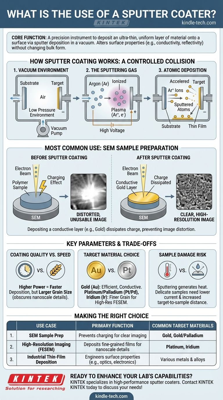
At its core, a sputter coater is a precision instrument used to deposit an ultra-thin, uniform layer of material onto a surface. This process, known as sputter deposition, is a foundational technique in modern science and engineering. It is used to create films ranging from just a few nanometers to several micrometers thick inside a vacuum chamber, fundamentally altering the properties of the substrate's surface.
Many advanced technologies and scientific analyses require modifying a material's surface properties—such as electrical conductivity or reflectivity—without changing its bulk form. A sputter coater provides a highly controllable and reliable method to apply this functional thin film.
How Sputter Coating Works: A Controlled Collision
The process is a physical vapor deposition (PVD) method that takes place under a controlled vacuum. The elegance of the technique lies in its use of momentum transfer.
The Vacuum Environment
First, the sample (the substrate) and the coating material (the target) are placed in a chamber, and the air is pumped out. This vacuum is critical to prevent contamination and to allow atoms to travel unimpeded from the target to the substrate.
The Sputtering Gas
An inert gas, typically argon, is then introduced into the chamber at a very low pressure. A high voltage is applied, which strips electrons from the argon atoms and creates an ionized gas, or plasma.
The Atomic Deposition
These positively charged argon ions are accelerated by an electric field and slam into the negatively charged target. This high-energy collision physically knocks, or "sputters," atoms off the target material. These ejected atoms travel through the vacuum and land on the substrate, gradually building up a thin, uniform film.
The Most Common Use: Preparing Samples for Electron Microscopy
While sputter coating has many industrial uses, its most frequent application in research labs is preparing samples for a Scanning Electron Electron Microscope (SEM).
The Challenge of Non-Conductive Samples
An SEM creates an image by scanning a surface with a focused beam of electrons. If the sample is non-conductive (e.g., a polymer, ceramic, or biological specimen), the electrons from the beam accumulate on its surface.
The "Charging" Effect
This buildup of static charge deflects the incoming electron beam, causing severe image distortion, unnatural brightness, and a complete loss of fine detail. The resulting image is often unusable for scientific analysis.
The Sputter Coater's Solution
By depositing a nanometer-thick layer of a conductive metal—most commonly gold—the sputter coater provides a path for this excess charge to dissipate. The coating is so thin that it preserves the sample's surface topography while rendering it conductive, enabling a clear, stable, and high-resolution image.
Understanding the Trade-offs and Key Parameters
The quality of the coating is not automatic. It depends on a careful balance of several process parameters, which must be tuned for the specific application.
Coating Quality vs. Deposition Speed
The sputter current and voltage directly impact how quickly the film is deposited. Higher power leads to a faster coating process but can also increase the grain size of the metallic film. For routine work this is fine, but for ultra-high-resolution imaging, a larger grain can obscure the very nanoscale details you want to see.
Target Material Choice
Gold is a popular choice because it is highly efficient to sputter and very conductive. However, for the highest-resolution microscopy, materials like platinum/palladium or iridium are often used because they produce a much finer, more uniform grain structure.
The Risk of Sample Damage
The sputtering process generates some heat. For robust samples this is not an issue, but delicate biological or polymer samples can be damaged. Lowering the sputter current and increasing the target-to-sample distance can mitigate this heating effect at the cost of a longer deposition time.
Making the Right Choice for Your Goal
The ideal sputter coating process is dictated entirely by your end goal.
- If your primary focus is routine SEM imaging of robust samples: A standard gold or gold/palladium coating at a relatively high current provides a fast, cost-effective solution for preventing charging.
- If your primary focus is ultra-high-resolution microscopy (FESEM): You must use a finer-grained (and often thinner) coating like platinum or iridium, applied at a lower current, to resolve nanoscale features without obscuring them.
- If your primary focus is industrial thin-film deposition (e.g., for optics or semiconductors): The choice of target material and all process parameters is strictly determined by the final electrical, optical, or magnetic properties required for the device.
Ultimately, a sputter coater is a powerful tool for precisely engineering a material's surface to either reveal its hidden details or enable entirely new functionality.
Summary Table:
| Key Use Case | Primary Function | Common Target Materials |
|---|---|---|
| SEM Sample Preparation | Prevents charging on non-conductive samples for clear imaging | Gold, Gold/Palladium |
| High-Resolution Imaging (FESEM) | Deposits fine-grained films to resolve nanoscale details | Platinum, Iridium |
| Industrial Thin-Film Deposition | Engineers surface properties for electronics & optics | Various metals & alloys |
Ready to enhance your lab's capabilities with precise thin-film deposition?
KINTEK specializes in high-performance sputter coaters and lab equipment, providing reliable solutions for your specific application—whether it's routine SEM sample preparation or advanced materials research. Our experts can help you select the ideal system to achieve superior results and improve your lab's efficiency.
Contact KINTEK today to discuss your needs and discover the right sputter coater for your laboratory!
Visual Guide
Related Products
- Custom CVD Diamond Coating for Lab Applications
- HFCVD Machine System Equipment for Drawing Die Nano-Diamond Coating
- Multifunctional Electrolytic Electrochemical Cell Water Bath Single Layer Double Layer
- Professional Cutting Tools for Carbon Paper Cloth Diaphragm Copper Aluminum Foil and More
- Chemical Vapor Deposition CVD Equipment System Chamber Slide PECVD Tube Furnace with Liquid Gasifier PECVD Machine
People Also Ask
- What are the different CVD coating? A Guide to Thermal CVD, PECVD, and Specialized Methods
- What is CVD coating used for? Hardening Tools & Building Semiconductors for Industry
- What are the types of CVD coating? A Guide to Choosing the Right Process
- What is CVD diamond coating? Grow a Super-Hard, High-Performance Diamond Layer
- What is the use of CVD coating? Enhance Durability and Functionality for Your Components


