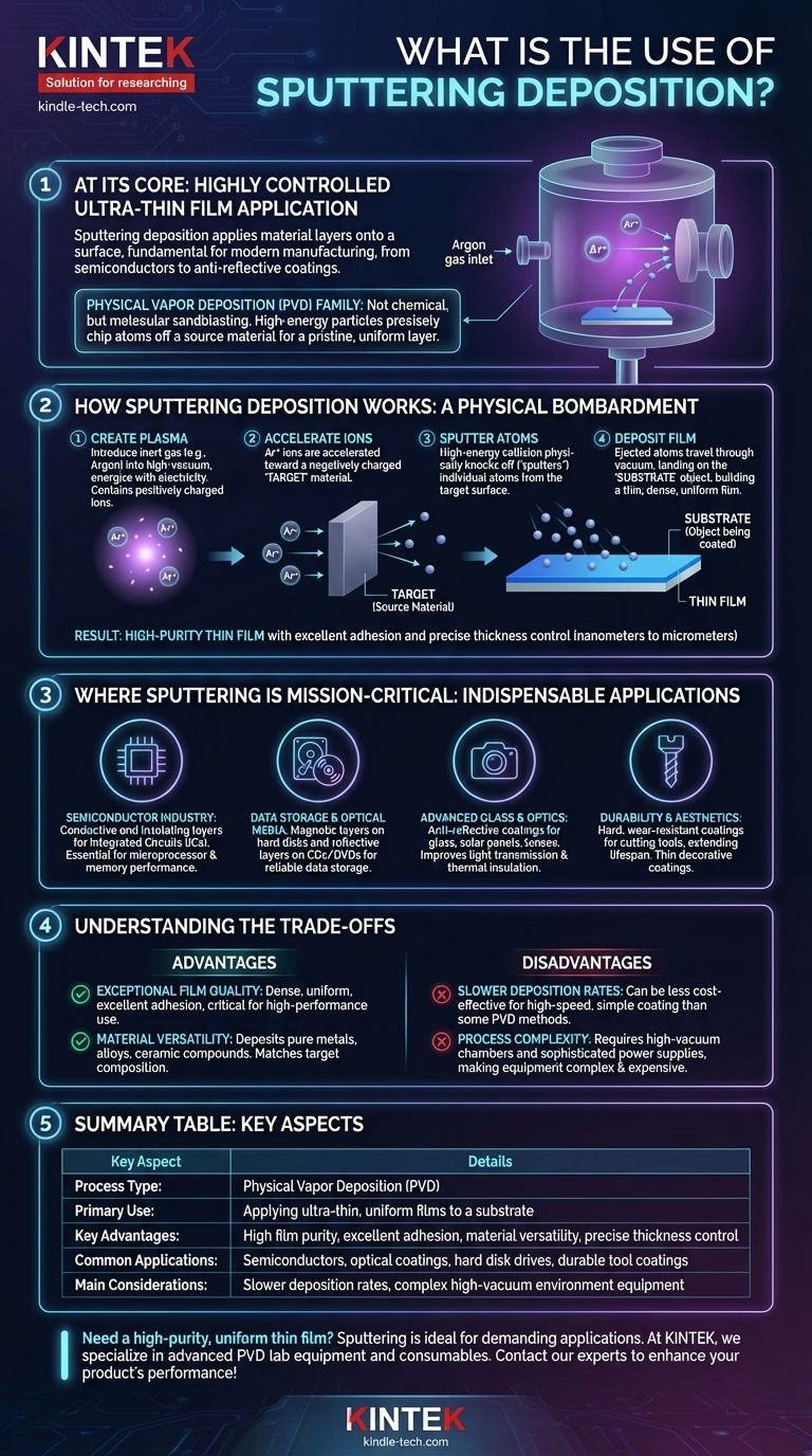
At its core, sputtering deposition is a highly controlled technique used to apply ultra-thin films of material onto a surface. This process is fundamental to modern manufacturing, enabling the creation of everything from the magnetic layers in computer hard disks and the complex circuitry in semiconductors to the anti-reflective coatings on eyeglasses and the durable finishes on cutting tools.
Sputtering is not a chemical coating but a physical one. Think of it as a form of molecular sandblasting, where high-energy particles are used to precisely chip atoms off a source material and deposit them as a pristine, uniform layer onto a target substrate.
How Sputtering Deposition Works
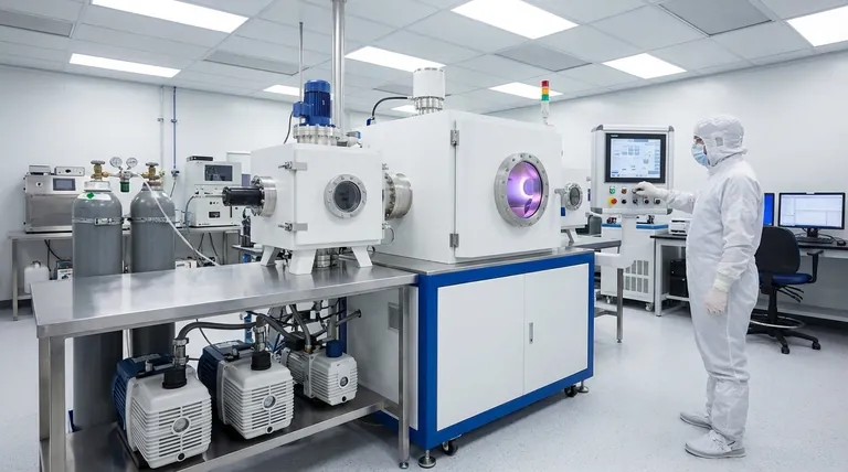
To understand why sputtering is so widely used, you first need to grasp its underlying mechanism. It's a process that belongs to a family of techniques called Physical Vapor Deposition (PVD), all of which occur in a high-vacuum environment.
The Core Principle: A Physical Bombardment
The entire process begins by creating a plasma, typically by introducing an inert gas like argon into a vacuum chamber and energizing it with electricity.
This plasma contains positively charged argon ions. These ions are accelerated toward a source material, known as the "target," which is given a negative electrical charge.
When these high-energy ions collide with the target, they physically knock off, or "sputter," individual atoms from its surface.
Key Components in the Process
These ejected atoms then travel through the vacuum chamber and land on the object being coated, called the "substrate."
Over time, these atoms build up on the substrate, forming a very thin, dense, and highly uniform film. The thickness can be controlled with extreme precision, from a few nanometers to several micrometers.
The Result: A High-Purity Thin Film
Because the process happens in a vacuum, there are very few contaminants. The result is a film with high purity and strong adhesion to the substrate, properties that are critical for high-performance applications.
Where Sputtering is Mission-Critical
The precision and versatility of sputtering have made it an indispensable process in numerous advanced industries.
In the Semiconductor Industry
Sputtering is used extensively to deposit the various conductive and insulating layers required to build an integrated circuit (IC). The ability to create flawless, uniform films is essential for the performance of microprocessors and memory chips.
For Data Storage and Optical Media
The magnetic layers on computer hard disks and the reflective layers on CDs and DVDs are created using sputtering. The process allows for the exact material composition and thickness needed to store and read data reliably.
On Advanced Glass and Optics
Sputtering is used to apply anti-reflective coatings to architectural glass, solar panels, and camera lenses. These coatings improve light transmission and efficiency. High-emissivity films are also applied to glass to improve thermal insulation.
For Durability and Aesthetics
Hard, wear-resistant coatings are applied to cutting tools and drill bits using sputtering, significantly extending their lifespan. It is also used for applying thin, decorative coatings to automotive parts and other consumer products.
Understanding the Trade-offs
No single technology is perfect for every scenario. While powerful, sputtering deposition has specific characteristics that make it suitable for some applications and less so for others.
Advantage: Exceptional Film Quality
The primary advantage of sputtering is the quality of the film. Sputtered films are typically very dense, uniform, and have excellent adhesion to the substrate, which is critical for demanding electronic and optical uses.
Advantage: Material Versatility
Sputtering can be used to deposit a vast range of materials, including pure metals, alloys, and even insulating ceramic compounds. The composition of the sputtered film very closely matches the composition of the target material.
Disadvantage: Slower Deposition Rates
Compared to some other PVD methods like thermal evaporation, sputtering can be a slower process. This can make it less cost-effective for applications where film quality is less critical than high-speed production.
Disadvantage: Process Complexity
Sputtering systems require high-vacuum chambers and sophisticated power supplies to generate and control the plasma. This makes the equipment more complex and expensive than some simpler coating methods.
Making the Right Choice for Your Goal
Selecting the right deposition technique depends entirely on your project's specific requirements for performance, material, and cost.
- If your primary focus is precision and film purity for electronics or optics: Sputtering is often the ideal choice due to its superior control over film properties and uniformity.
- If your primary focus is coating a complex alloy or compound: Sputtering excels at transferring the target material's exact composition to the substrate without altering it.
- If your primary focus is high-speed, simple metal coating at the lowest cost: You might investigate other PVD methods like thermal evaporation, which can be faster for some materials.
Ultimately, sputtering deposition is a foundational technology that enables the performance and reliability of countless devices we depend on every day.
Summary Table:
| Key Aspect | Details |
|---|---|
| Process Type | Physical Vapor Deposition (PVD) |
| Primary Use | Applying ultra-thin, uniform films to a substrate |
| Key Advantages | High film purity, excellent adhesion, material versatility, precise thickness control |
| Common Applications | Semiconductors, optical coatings, hard disk drives, durable tool coatings |
| Main Considerations | Slower deposition rates, complex equipment requiring a high-vacuum environment |
Need a high-purity, uniform thin film for your lab equipment or product? Sputtering deposition is ideal for demanding applications in semiconductors, optics, and durable coatings. At KINTEK, we specialize in advanced lab equipment and consumables for precise Physical Vapor Deposition. Our experts can help you select the right sputtering solution to enhance your product's performance and reliability. Contact our team today to discuss your specific coating requirements!
Visual Guide
Related Products
- Chemical Vapor Deposition CVD Equipment System Chamber Slide PECVD Tube Furnace with Liquid Gasifier PECVD Machine
- RF PECVD System Radio Frequency Plasma-Enhanced Chemical Vapor Deposition RF PECVD
- Customer Made Versatile CVD Tube Furnace Chemical Vapor Deposition Chamber System Equipment
- Custom CVD Diamond Coating for Lab Applications
- Aluminized Ceramic Evaporation Boat for Thin Film Deposition
People Also Ask
- What are the core advantages of PE-CVD in OLED encapsulation? Protect Sensitive Layers with Low-Temp Film Deposition
- Why is Chemical Vapor Deposition (CVD) equipment uniquely suited for constructing hierarchical superhydrophobic structures?
- What are the processes of vapor phase deposition? Understand CVD vs. PVD for Superior Thin Films
- How are carbon nanotubes grown? Master Scalable Production with Chemical Vapor Deposition
- What types of substrates are used in CVD to facilitate graphene films? Optimize Graphene Growth with the Right Catalyst


