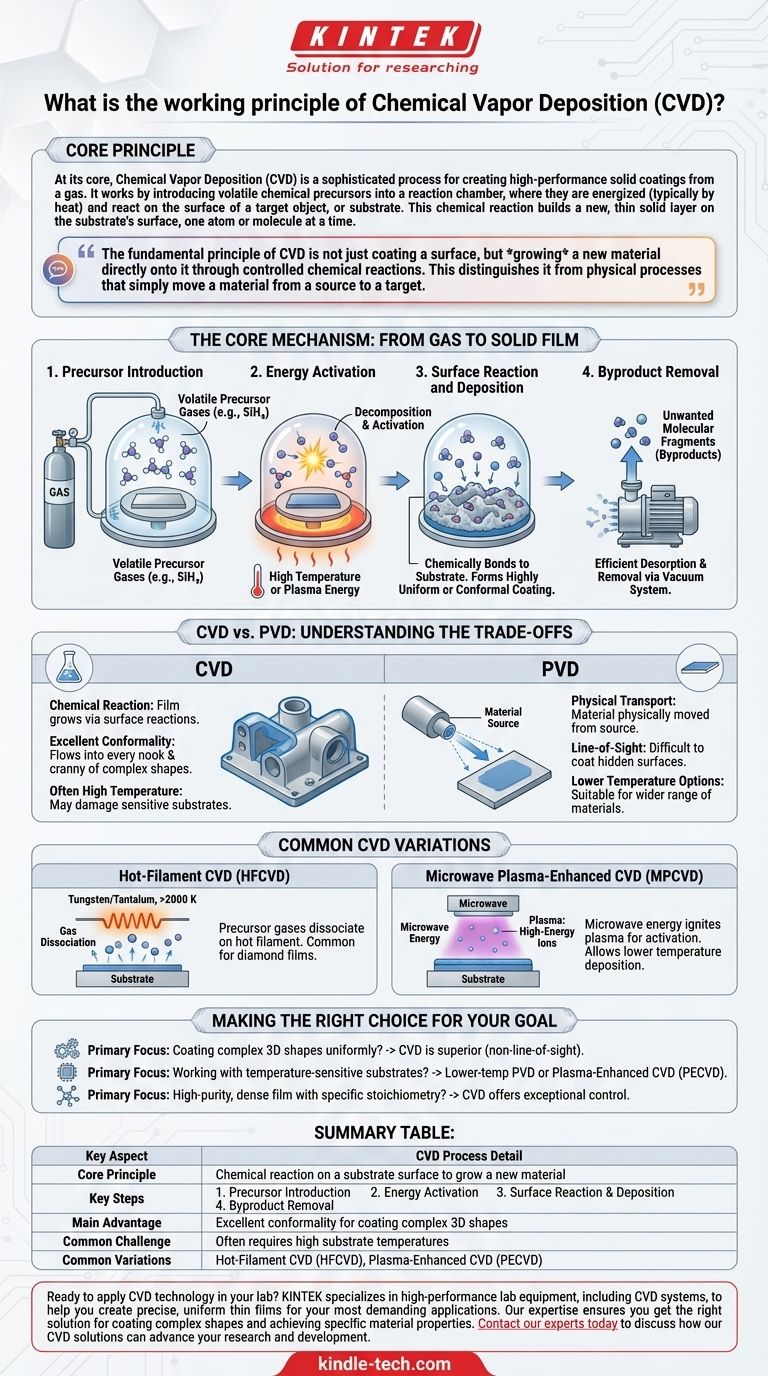
At its core, Chemical Vapor Deposition (CVD) is a sophisticated process for creating high-performance solid coatings from a gas. It works by introducing volatile chemical precursors into a reaction chamber, where they are energized (typically by heat) and react on the surface of a target object, or substrate. This chemical reaction builds a new, thin solid layer on the substrate's surface, one atom or molecule at a time.
The fundamental principle of CVD is not just coating a surface, but growing a new material directly onto it through controlled chemical reactions. This distinguishes it from physical processes that simply move a material from a source to a target.
The Core Mechanism: From Gas to Solid Film
To truly understand CVD, we must break it down into a sequence of distinct steps. Each step is critical for forming a high-quality, uniform thin film.
Step 1: Precursor Introduction
The process begins by injecting one or more volatile precursor gases into a reaction chamber, which is often held under a vacuum. These precursors are gaseous molecules that contain the specific chemical elements needed for the final coating.
For example, to deposit silicon, a gas like silane (SiH₄) might be used. For more complex materials, organometallic compounds are common.
Step 2: Energy Activation
The precursor gases do not react on their own. They must be activated by an external energy source. The most common method is heating the substrate to a specific reaction temperature.
This thermal energy causes the precursor gas molecules to decompose or break down into more reactive chemical species. Other methods, like using a hot filament or microwave plasma, can also provide this activation energy.
Step 3: Surface Reaction and Deposition
The reactive gas species adsorb, or land, onto the hot substrate surface. Once there, they undergo chemical reactions with the surface and with each other.
These reactions form a stable, solid material that chemically bonds to the substrate. This process occurs across the entire exposed surface, allowing the film to build up layer by layer, resulting in a highly uniform or conformal coating.
Step 4: Byproduct Removal
The chemical reactions often create unwanted molecular fragments, known as byproducts. For a clean film to form, these byproducts must be efficiently desorbed from the surface and removed from the chamber by the vacuum system.
Understanding the Trade-offs: CVD vs. PVD
CVD is often compared to Physical Vapor Deposition (PVD). Understanding their differences is key to appreciating CVD's unique strengths and weaknesses.
Chemical Reaction vs. Physical Transport
The defining difference is that CVD is a chemical process, while PVD is a physical one.
In CVD, the coating is a new material formed by reactions on the substrate. In PVD (like sputtering or evaporation), the source material is physically blasted or boiled into a vapor of atoms, which then travel in a line-of-sight path and condense on the substrate.
Coating Conformality
Because CVD relies on a gas that can flow into every nook and cranny of a complex part, it excels at producing highly uniform coatings on intricate 3D shapes.
PVD is a line-of-sight process, making it difficult to coat hidden surfaces or the inside of deep trenches without complex part manipulation.
Temperature and Material Limitations
Traditional CVD processes often require very high substrate temperatures (hundreds or thousands of degrees Celsius) to drive the chemical reactions. This can damage or alter temperature-sensitive substrates like plastics or certain metal alloys.
PVD can often be performed at much lower temperatures, making it suitable for a wider range of materials.
Common CVD Variations
The basic principle of CVD can be adapted by changing how the activation energy is supplied. This has led to several specialized techniques.
Hot-Filament CVD (HFCVD)
In HFCVD, a metal filament made of a refractory metal like tungsten or tantalum is heated to over 2000 K. The precursor gases dissociate as they pass over this intensely hot filament, creating the reactive species needed for deposition.
This method is common for growing diamond films, but a major drawback is that the filament itself can degrade over time.
Microwave Plasma-Enhanced CVD (MPCVD)
This technique uses microwave energy to ignite the precursor gases into a plasma—a high-energy state of matter containing ions and reactive molecular fragments.
The plasma provides the activation energy for the reactions, often allowing deposition to occur at a much lower overall gas temperature. This makes it a valuable method for coating more temperature-sensitive materials.
Making the Right Choice for Your Goal
Selecting a deposition method requires aligning the process capabilities with your primary objective.
- If your primary focus is coating complex 3D shapes uniformly: CVD is often the superior choice due to its non-line-of-sight, gas-phase nature.
- If your primary focus is working with temperature-sensitive substrates: A lower-temperature PVD process or a specialized Plasma-Enhanced CVD (PECVD) is likely the necessary approach.
- If your primary focus is creating a high-purity, dense film with specific stoichiometry: CVD offers exceptional control over the final material's chemistry through precise management of the precursor gases.
Ultimately, understanding the fundamental principles of deposition empowers you to select the technology that will most effectively achieve your desired material properties.
Summary Table:
| Key Aspect | CVD Process Detail |
|---|---|
| Core Principle | Chemical reaction on a substrate surface to grow a new material |
| Key Steps | 1. Precursor Introduction 2. Energy Activation 3. Surface Reaction & Deposition 4. Byproduct Removal |
| Main Advantage | Excellent conformality for coating complex 3D shapes |
| Common Challenge | Often requires high substrate temperatures |
| Common Variations | Hot-Filament CVD (HFCVD), Plasma-Enhanced CVD (PECVD) |
Ready to apply CVD technology in your lab?
KINTEK specializes in high-performance lab equipment, including CVD systems, to help you create precise, uniform thin films for your most demanding applications. Our expertise ensures you get the right solution for coating complex shapes and achieving specific material properties.
Contact our experts today to discuss how our CVD solutions can advance your research and development.
Visual Guide
Related Products
- Chemical Vapor Deposition CVD Equipment System Chamber Slide PECVD Tube Furnace with Liquid Gasifier PECVD Machine
- RF PECVD System Radio Frequency Plasma-Enhanced Chemical Vapor Deposition RF PECVD
- Microwave Plasma Chemical Vapor Deposition MPCVD Machine System Reactor for Lab and Diamond Growth
- Customer Made Versatile CVD Tube Furnace Chemical Vapor Deposition Chamber System Equipment
- 915MHz MPCVD Diamond Machine Microwave Plasma Chemical Vapor Deposition System Reactor
People Also Ask
- What are the processes of vapor phase deposition? Understand CVD vs. PVD for Superior Thin Films
- How are carbon nanotubes grown? Master Scalable Production with Chemical Vapor Deposition
- How expensive is chemical vapor deposition? Understanding the True Cost of High-Performance Coating
- What is the chemical vapor deposition growth process? Build Superior Thin Films from the Atom Up
- What are the advantages of chemical vapor deposition? Achieve Superior Thin Films for Your Lab


