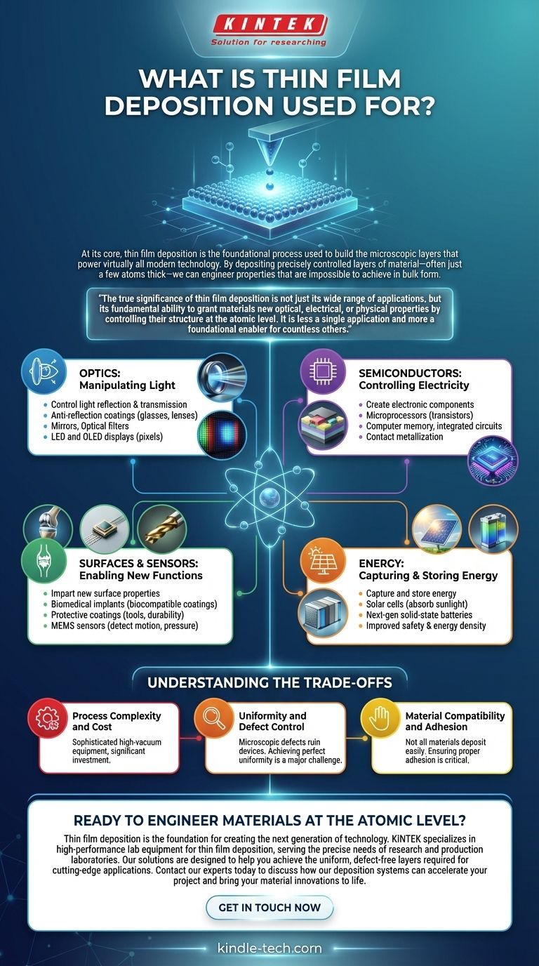
At its core, thin film deposition is the foundational process used to build the microscopic layers that power virtually all modern technology. It is the technique responsible for manufacturing semiconductor chips for computers, creating anti-reflection coatings for eyeglasses and camera lenses, and producing the vibrant pixels in LED and OLED displays. By depositing precisely controlled layers of material—often just a few atoms thick—we can engineer properties that are impossible to achieve in bulk form.
The true significance of thin film deposition is not just its wide range of applications, but its fundamental ability to grant materials new optical, electrical, or physical properties by controlling their structure at the atomic level. It is less a single application and more a foundational enabler for countless others.
The Core Principle: Engineering Properties at the Nanoscale
The central goal of thin film deposition is to build a material layer by layer, giving engineers precise control over its function. This process allows us to create structures that manipulate light, control the flow of electricity, or protect a surface in ways a solid piece of the same material never could.
Manipulating Light (Optics)
One of the most common uses of thin films is to control the behavior of light. By stacking ultra-thin layers with different refractive indices, we can fine-tune how light is reflected, transmitted, or absorbed.
This principle is behind anti-reflection coatings on prescription glasses and camera lenses, which maximize light transmission for clearer vision. It's also how mirrors and optical filters are made, designed to reflect or pass only specific wavelengths of light.
In LED and OLED displays, thin films are the active components that emit light, with their thickness and composition determining the color and brightness of each pixel.
Controlling Electricity (Semiconductors)
The modern electronics industry is built on thin film deposition. The microprocessors in your phone and computer are composed of billions of transistors, each one built by depositing and etching a complex stack of thin films.
These layers create the essential components of a transistor, alternating between conductive, insulating, and semiconducting materials. The precise thickness of an insulating layer, for example, can determine if a transistor functions correctly or fails.
This applies to everything from computer memory and integrated circuits to the contact metallization that connects all the components on a chip.
Enabling New Functions (Surfaces and Sensors)
Thin films can also impart entirely new properties to the surface of an object. This is critical in a wide range of industrial and medical applications.
For instance, biomedical implants like pacemakers or artificial joints are coated with thin, biocompatible films to prevent the body from rejecting them.
Hard, protective coatings are deposited on cutting tools and drill bits to increase their lifespan and durability. Similarly, thin films form the sensing layers in micro-electro-mechanical systems (MEMS) that detect everything from motion in your phone to pressure and temperature in industrial settings.
Capturing and Storing Energy
Thin film technology is vital for renewable energy and energy storage. The active layers in most solar cells are thin films designed to efficiently absorb sunlight and convert it into electricity.
Likewise, researchers are using thin film deposition to develop next-generation solid-state batteries, which promise higher energy density and improved safety by replacing the liquid electrolyte with a solid thin film.
Understanding the Trade-offs
While incredibly powerful, thin film deposition is a highly complex and sensitive process. Understanding its challenges is key to appreciating its role.
Process Complexity and Cost
Creating uniform films just atoms thick requires sophisticated equipment operating in a high vacuum. These deposition systems are expensive to acquire and maintain, making the process a significant investment.
Uniformity and Defect Control
Even a single misplaced atom or microscopic dust particle can create a defect that ruins a semiconductor device or an optical coating. Achieving perfect uniformity and purity across an entire surface (like a silicon wafer) is a major, ongoing engineering challenge.
Material Compatibility and Adhesion
Not all materials can be easily deposited as a thin film. Furthermore, ensuring the deposited film sticks properly to the underlying substrate (adhesion) without peeling or cracking is a critical hurdle that requires careful material selection and process control.
Making the Right Choice for Your Goal
The application of thin film deposition is defined by the specific property you need to engineer. The goal dictates the material, thickness, and deposition method.
- If your primary focus is electronics: You will use deposition to create the complex, multi-layered transistor structures that form the basis of microchips.
- If your primary focus is optics: You will use deposition to stack layers that manipulate light for anti-reflection, filtering, or display purposes.
- If your primary focus is a physical product: You will use deposition to apply a surface coating that provides durability, biocompatibility, or chemical resistance.
- If your primary focus is energy: You will use deposition to create the active layers that convert light to electricity in solar cells or enable ion transport in batteries.
Ultimately, thin film deposition is the invisible art of building our modern world, one atomic layer at a time.
Summary Table:
| Application Area | Key Functions | Common Examples |
|---|---|---|
| Optics | Control light reflection & transmission | Anti-reflection coatings, mirrors, LED/OLED displays |
| Semiconductors | Create electronic components | Microprocessors, computer memory, integrated circuits |
| Surfaces & Sensors | Impart new surface properties | Biomedical implants, protective coatings, MEMS sensors |
| Energy | Capture and store energy | Solar cells, solid-state batteries |
Ready to engineer materials at the atomic level?
Thin film deposition is the foundation for creating the next generation of technology. Whether you are developing advanced semiconductors, precision optics, durable surface coatings, or innovative energy solutions, the right equipment is critical to your success.
KINTEK specializes in high-performance lab equipment for thin film deposition, serving the precise needs of research and production laboratories. Our solutions are designed to help you achieve the uniform, defect-free layers required for cutting-edge applications.
Contact our experts today to discuss how our deposition systems can accelerate your project and bring your material innovations to life.
Visual Guide
Related Products
- Aluminized Ceramic Evaporation Boat for Thin Film Deposition
- Tungsten Evaporation Boat for Thin Film Deposition
- Electron Beam Evaporation Coating Oxygen-Free Copper Crucible and Evaporation Boat
- Molybdenum Tungsten Tantalum Evaporation Boat for High Temperature Applications
- HFCVD Machine System Equipment for Drawing Die Nano-Diamond Coating
People Also Ask
- What is the chemical method for thin film deposition? Build Films from the Molecular Level Up
- What is the source of evaporation for thin film? Choosing Between Thermal and E-Beam Methods
- What are the alternatives to sputtering? Choose the Right Thin Film Deposition Method
- Why is an alumina boat selected for catalyst precursors? Ensure Sample Purity at 1000 °C
- What is the widely used boat made of in thermal evaporation? Choosing the Right Material for High-Purity Deposition


