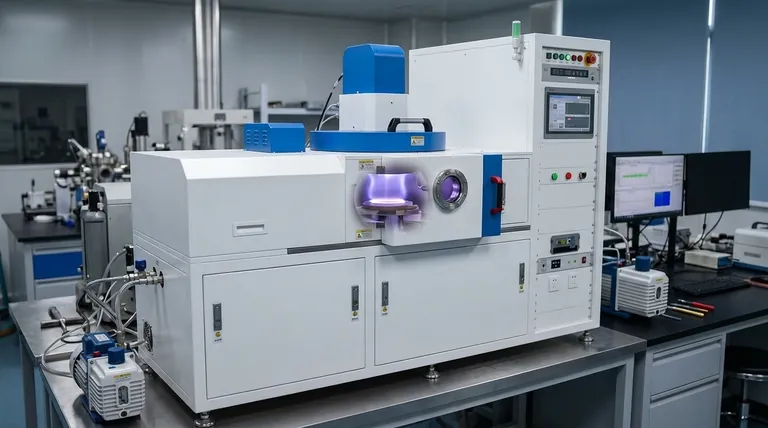
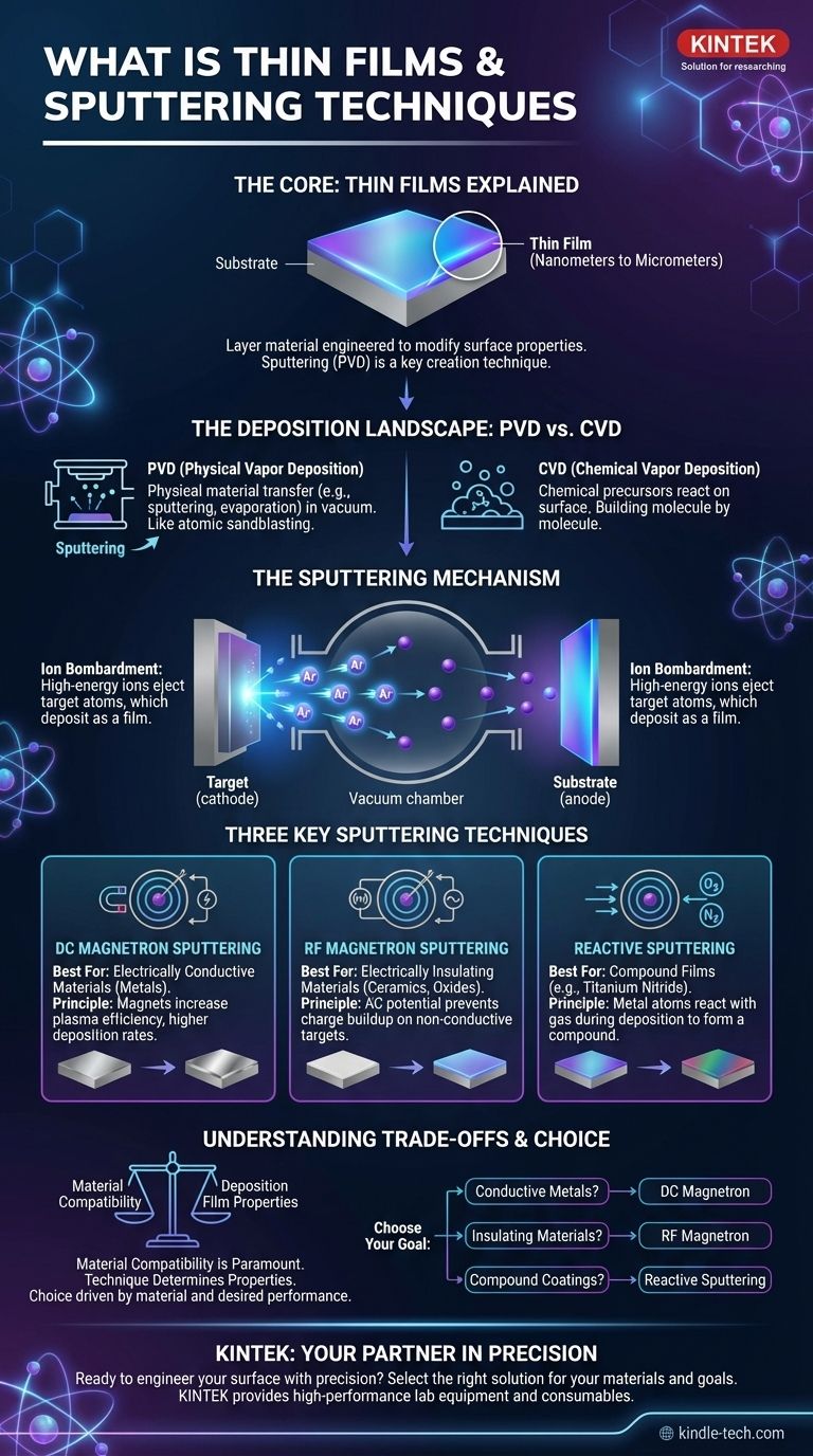
At its core, a thin film is a layer of material ranging from a few nanometers to several micrometers in thickness, engineered to modify the surface properties of an object. Sputtering is a dominant technique for creating these films and falls under the category of Physical Vapor Deposition (PVD). It works by bombarding a source material (a "target") with energetic ions, which ejects or "sputters" atoms from the target that then deposit onto a substrate, forming the desired thin film.
Understanding sputtering isn't just about knowing the process; it's about recognizing it as a tool for atomic-level construction. The specific technique you choose dictates which materials you can use and directly engineers the final properties of your film, from its electrical conductivity to its mechanical hardness.
The Landscape of Thin Film Deposition
To understand sputtering, you must first see where it fits within the broader field of thin film creation. The methods are generally divided into two major families based on how they transport material to the substrate.
The Two Major Families: PVD and CVD
The two primary deposition techniques are Physical Vapor Deposition (PVD) and Chemical Vapor Deposition (CVD).
PVD processes, including sputtering, use physical mechanisms like high-energy bombardment or evaporation to transfer material from a source to a substrate in a vacuum. Think of it as an atomic-scale sandblasting and coating process.
CVD processes use volatile precursor chemicals that react or decompose on the substrate's surface to form the film. This is more akin to building the film layer molecule by molecule through controlled chemical reactions.
Where Sputtering Fits
Sputtering is a PVD technique. It is distinct from other PVD methods like evaporation, which involves simply heating a material until it turns into a vapor. Sputtering is a more energetic process, leading to denser and more adherent films.
A Deeper Look at Sputtering Techniques
All sputtering operates on the same basic principle, but different variations have been developed to handle different materials and achieve specific film characteristics.
The Core Mechanism: Ion Bombardment
The process begins by creating a low-pressure plasma, typically from an inert gas like Argon. A high voltage is applied between the substrate and the target material, causing the gas to ionize.
These positively charged Argon ions are accelerated into the negatively charged target. The high-energy impact physically knocks atoms loose from the target, which then travel through the vacuum chamber and condense on the substrate as a thin film.
DC Magnetron Sputtering
This is the workhorse technique for depositing electrically conductive materials, such as metals.
It uses powerful magnets behind the target (a "magnetron") to trap electrons in a magnetic field. This greatly increases the efficiency of the ionization process, resulting in a more stable plasma and higher deposition rates compared to simple DC sputtering.
RF Magnetron Sputtering
When you need to deposit electrically insulating materials (dielectrics), like ceramics or oxides, DC sputtering fails. Charge builds up on the surface of the insulating target, effectively stopping the ion bombardment.
RF (Radio Frequency) sputtering solves this by using an alternating AC potential. The rapid switching of the electric field prevents charge accumulation, allowing for the continuous sputtering of non-conductive materials.
Reactive Sputtering
This technique is used to create compound films. It involves sputtering a metallic target in a vacuum chamber that contains a mixture of inert and reactive gases (like oxygen or nitrogen).
As the sputtered metal atoms travel toward the substrate, they react with the gas to form a compound. For example, sputtering a titanium target in a nitrogen atmosphere creates a hard, gold-colored Titanium Nitride (TiN) coating.
Understanding the Trade-offs
Choosing a sputtering technique is a matter of balancing material requirements, process complexity, and desired film properties. The technique is not just a delivery method; it is a primary factor in the film's performance.
Material Compatibility Is Paramount
The most critical factor is the electrical conductivity of your target material. DC sputtering is simpler and generally faster, but it is strictly limited to conductive targets. RF sputtering offers the versatility to deposit virtually any material but is often slower and requires more complex power supplies.
Deposition Control and Film Quality
Sputtering provides excellent control over film thickness and uniformity across large areas. Because the sputtered atoms have high kinetic energy, they create films that are typically much denser and have stronger adhesion to the substrate compared to thermal evaporation.
The Technique Determines the Properties
The deposition parameters—such as gas pressure, power, and substrate temperature—have a direct and significant impact on the film's final characteristics. Properties like crystal structure, internal stress, density, and resistivity are all determined by how the film is grown.
Making the Right Choice for Your Goal
Your decision must be driven by the material you intend to deposit and the performance you require from the final film.
- If your primary focus is depositing conductive metals like aluminum or titanium: DC magnetron sputtering is your most efficient and cost-effective choice.
- If your primary focus is depositing insulating materials like silicon dioxide (SiO2) or ceramics: RF magnetron sputtering is the necessary method to overcome target charging issues.
- If your primary focus is creating hard, functional compound coatings like titanium nitride (TiN): Reactive sputtering gives you the power to synthesize the compound material during the deposition process itself.
By understanding these fundamental techniques and their trade-offs, you can select the right process to precisely engineer the properties of your surface.
Summary Table:
| Technique | Best For | Key Principle |
|---|---|---|
| DC Magnetron Sputtering | Electrically Conductive Materials (Metals) | Uses magnets to increase plasma efficiency for high deposition rates. |
| RF Magnetron Sputtering | Electrically Insulating Materials (Ceramics, Oxides) | Uses radio frequency to prevent charge buildup on non-conductive targets. |
| Reactive Sputtering | Compound Films (e.g., Titanium Nitride) | Sputters a metal target in a reactive gas atmosphere to form a compound. |
Ready to engineer your surface with precision? The right sputtering technique is critical for achieving the desired electrical, mechanical, and chemical properties in your thin film. KINTEK specializes in providing high-performance lab equipment and consumables for all your thin film deposition needs, from research to production.
Let our experts help you select the ideal sputtering solution for your specific materials and goals.
Contact KINTEK today to discuss your project and discover how we can enhance your laboratory's capabilities.
Visual Guide
Related Products
- Spark Plasma Sintering Furnace SPS Furnace
- Vacuum Induction Melting Spinning System Arc Melting Furnace
- Chemical Vapor Deposition CVD Equipment System Chamber Slide PECVD Tube Furnace with Liquid Gasifier PECVD Machine
- Customer Made Versatile CVD Tube Furnace Chemical Vapor Deposition Chamber System Equipment
People Also Ask
- What technical advantages does a Spark Plasma Sintering (SPS) furnace offer for LZP ceramics? Enhance Ionic Conductivity
- What are the advantages of CAMI/SPS for W-Cu composite preparation? Reduce cycles from hours to seconds.
- What is the mechanism of SPS process? A Deep Dive into Rapid, Low-Temperature Sintering
- What is the theory of spark plasma sintering? A Guide to Rapid, Low-Temperature Densification
- What is the difference between spark plasma sintering and flash sintering? A Guide to Advanced Sintering Methods


