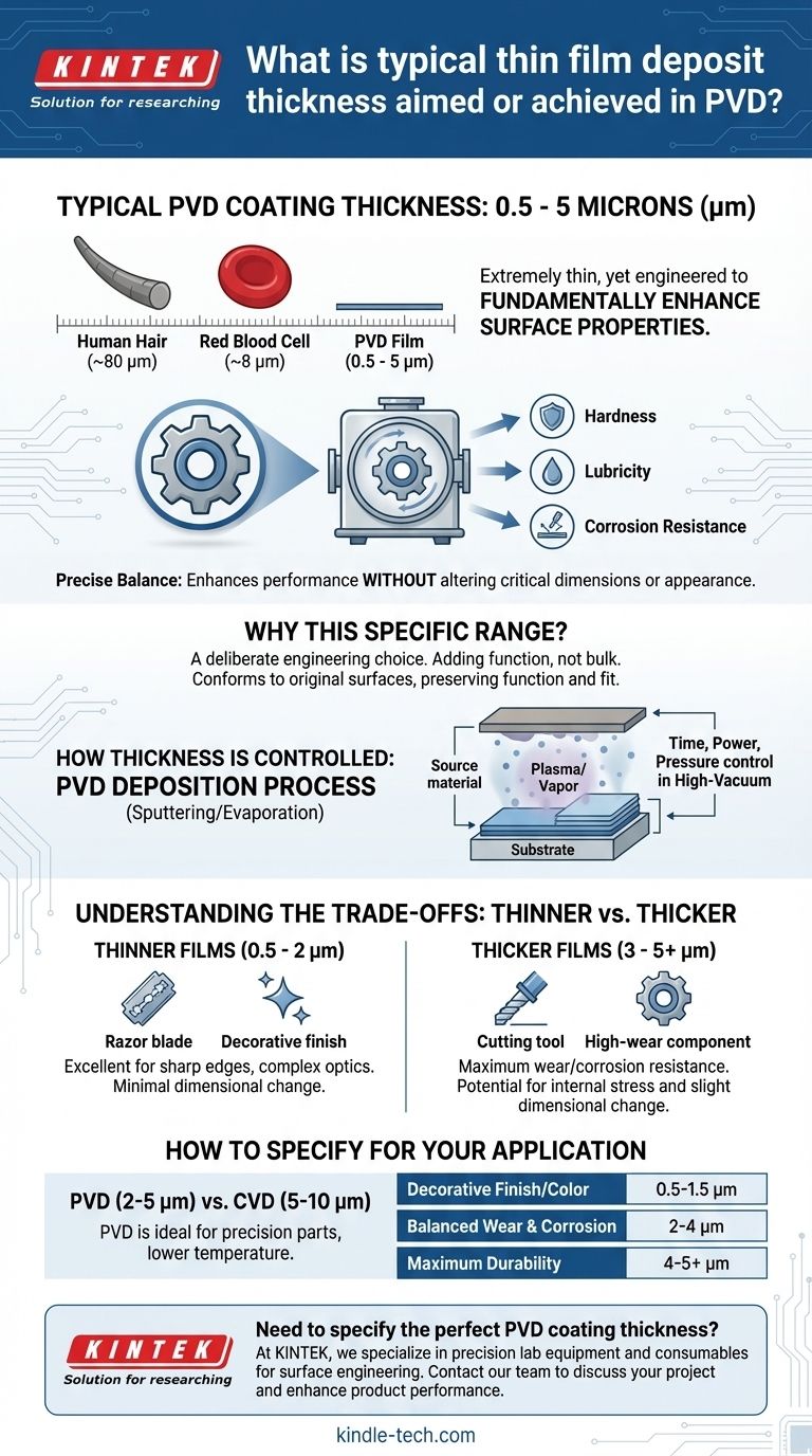
The typical thickness of a Physical Vapor Deposition (PVD) coating is between 0.5 and 5 microns (µm). This extremely thin film is engineered to be thick enough to fundamentally enhance a material's surface properties—such as hardness, lubricity, and corrosion resistance—while being thin enough to avoid altering the component's critical dimensions or appearance.
The thickness of a PVD coating is not an arbitrary value but a critical design parameter. It represents a precise balance—thick enough to provide desired performance, yet so thin that it preserves the part's original engineering tolerances and surface finish.
Why This Specific Thickness Range?
The decision to use a coating in the micron or sub-micron range is a deliberate engineering choice driven by the goals of the PVD process. It's about adding function without adding bulk.
The Scale of PVD Coatings
To understand this scale, consider that a human hair is about 80 microns thick and a red blood cell is about 8 microns. A typical PVD coating is often thinner than a single blood cell.
This minimal thickness is the key to its utility. It allows engineers to apply functional coatings to precision components without having to redesign the part to account for the added material.
Achieving Performance Without Altering Dimensions
The primary goal of PVD is to impart new mechanical, chemical, or optical properties to a substrate's surface.
A few microns of a hard material like Titanium Nitride (TiN) or Zirconium Nitride (ZrN) is sufficient to dramatically increase surface hardness and wear resistance.
Because the layer is so thin, it conforms to the original surface without rounding sharp edges or filling in crucial textures, preserving the part's intended function and fit.
How Thickness is Controlled and Selected
The final thickness of a PVD coating is not an accident. It is meticulously controlled in a high-vacuum environment to meet the specific demands of the application.
The Deposition Process
PVD methods like sputtering or evaporation work by transforming a solid source material into atomic particles within a vacuum chamber.
These particles travel and deposit onto the substrate, building the film layer by layer. The thickness is precisely controlled by managing process parameters like time, power, and pressure.
Targeting Specific Properties
The ideal thickness is chosen based on the desired outcome. A decorative coating might only need to be 1 micron thick to achieve a specific color and luster.
In contrast, a cutting tool subjected to extreme wear and heat may require a thicker coating of 4-5 microns to maximize its operational life.
Understanding the Trade-offs
While PVD is a versatile process, selecting a thickness involves balancing competing factors. It is not always a case of "thicker is better."
Thinner vs. Thicker Films
Thinner films (0.5 - 2 µm) are excellent for components with very sharp edges (like razor blades) or complex optical requirements. They add minimal dimensional change but may offer less durability in high-wear environments.
Thicker films (3 - 5+ µm) provide maximum wear and corrosion resistance. However, they can build up internal stress, potentially leading to adhesion issues, and may begin to slightly alter the component's dimensions if not applied correctly.
PVD vs. Other Processes (like CVD)
It is useful to compare PVD to Chemical Vapor Deposition (CVD), another common coating method.
PVD coatings are typically thinner (2-5 microns) than CVD coatings (5-10 microns). The lower process temperature and thinner nature of PVD make it ideal for precision-machined parts that cannot tolerate dimensional changes or high heat.
Line-of-Sight Limitations
PVD is a "line-of-sight" process, meaning the coating material travels in a straight line from the source to the substrate.
Achieving a perfectly uniform thickness on highly complex, three-dimensional parts can be a challenge and may require sophisticated part rotation and fixturing within the coating chamber.
How to Specify Thickness for Your Application
Choosing the right thickness requires you to clearly define your primary objective. Consult with your coating provider, but use these general guidelines as a starting point.
- If your primary focus is a decorative finish or specific color: A thinner coating (e.g., 0.5 to 1.5 microns) is often sufficient and cost-effective.
- If your primary focus is balanced wear and corrosion resistance: Target the middle of the range (e.g., 2 to 4 microns) for a robust, all-around performance profile.
- If your primary focus is maximum durability for high-wear tools: Aim for the upper end of the typical range (e.g., 4 to 5 microns), but confirm the potential dimensional impact with your provider.
Ultimately, selecting the right PVD coating thickness is a deliberate engineering choice that directly impacts the performance and lifespan of your component.
Summary Table:
| Application Goal | Typical Thickness Range | Key Benefit |
|---|---|---|
| Decorative Finish / Color | 0.5 - 1.5 µm | Cost-effective, minimal dimensional change |
| Balanced Wear & Corrosion Resistance | 2 - 4 µm | Robust, all-around performance |
| Maximum Durability (e.g., Cutting Tools) | 4 - 5+ µm | Enhanced wear resistance and lifespan |
Need to specify the perfect PVD coating thickness for your components?
At KINTEK, we specialize in precision lab equipment and consumables for surface engineering. Our experts can help you select the ideal coating parameters to achieve the hardness, lubricity, and corrosion resistance your application demands—without compromising dimensional accuracy.
Contact our team today to discuss your project and discover how KINTEK's solutions can enhance your product's performance and longevity.
Visual Guide
Related Products
- Molybdenum Tungsten Tantalum Evaporation Boat for High Temperature Applications
- RF PECVD System Radio Frequency Plasma-Enhanced Chemical Vapor Deposition RF PECVD
- Hemispherical Bottom Tungsten Molybdenum Evaporation Boat
- Aluminized Ceramic Evaporation Boat for Thin Film Deposition
- Tungsten Evaporation Boat for Thin Film Deposition
People Also Ask
- What is the meaning of thermal evaporation? A Guide to Simple, Cost-Effective Thin Film Coating
- What is vacuum thermal evaporation? A Guide to High-Purity Thin Film Deposition
- What is the difference between sputtering and thermal evaporation? Choose the Right PVD Method for Your Thin Film
- What is the widely used boat made of in thermal evaporation? Choosing the Right Material for High-Purity Deposition
- What are the drawbacks of thermal evaporation? Understanding the Limitations for High-Performance Applications