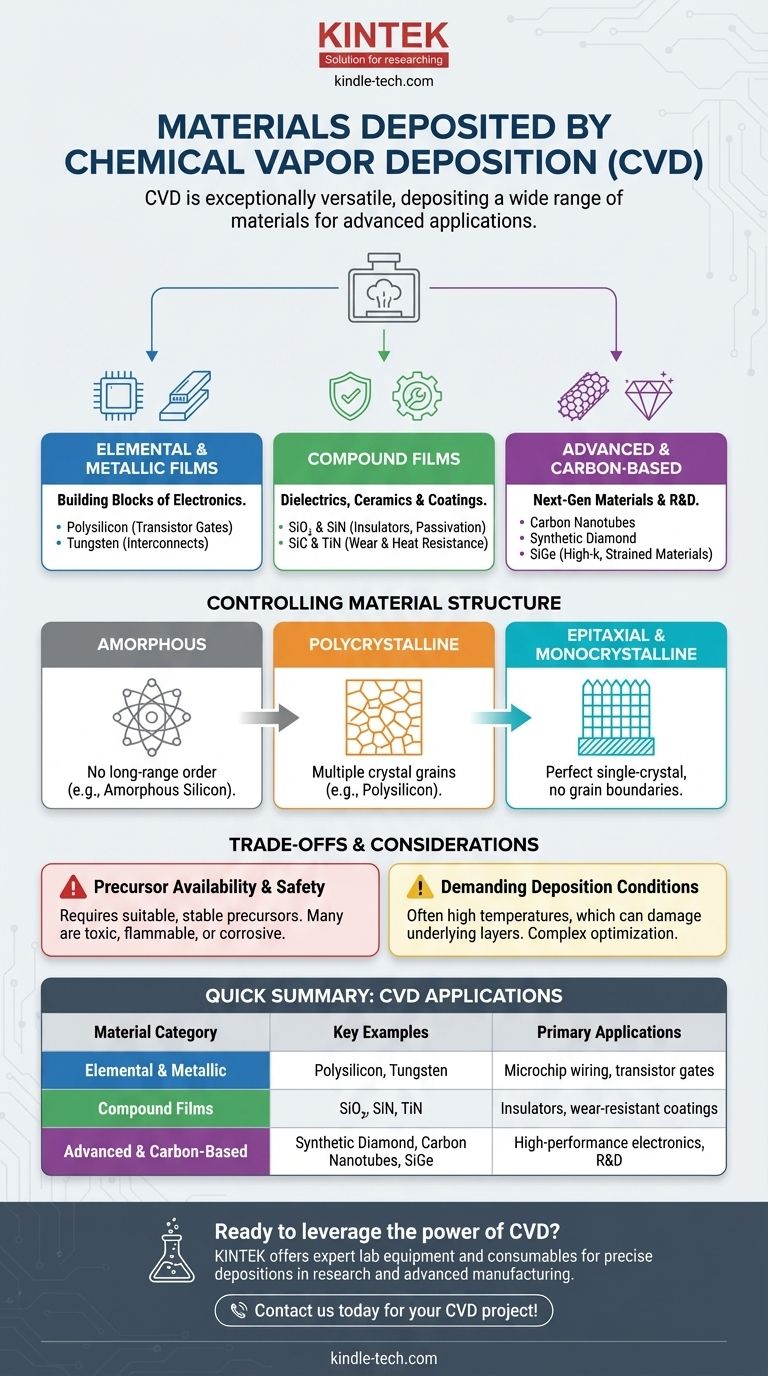
At its core, Chemical Vapor Deposition (CVD) is remarkably versatile, capable of depositing an exceptionally wide range of materials. The process is not limited to a single class of substance; instead, it can be used to create thin films of elemental materials like silicon and tungsten, compound insulators and ceramics like silicon nitride and titanium nitride, and even exotic materials like synthetic diamond and carbon nanotubes.
The true power of CVD is not just the extensive list of materials it can deposit, but its precise control over the material’s final structural form—from amorphous to perfect single-crystal—and its resulting physical properties. This makes it an indispensable tool for advanced manufacturing.
The Three Pillars of CVD Materials
The materials deposited by CVD can be broadly organized into three fundamental categories, each serving critical functions in technology and industry.
Elemental and Metallic Films
These are often the building blocks of electronic devices. CVD is a primary method for depositing conductive films that form the wiring and components of microchips.
Common examples include polysilicon, which is fundamental for creating transistor gates, and metals like tungsten, used to fill vias and create reliable electrical interconnects between layers in a semiconductor device.
Compound Films: Dielectrics and Ceramics
This is arguably the most diverse category. CVD excels at creating compound materials that act as insulators (dielectrics) or protective, hard coatings (ceramics).
In microelectronics, films like silicon dioxide (SiO₂) and silicon nitride (SiN) are ubiquitous, serving as insulators, passivation layers, and etch masks. Complex stacks like oxide-nitride-oxide (ONO) are also standard.
For industrial applications, hard ceramics like silicon carbide (SiC) and titanium nitride (TiN) are deposited on machine tools, engine components, and turbine blades to provide extreme wear and heat resistance.
Advanced and Carbon-Based Materials
CVD is at the forefront of materials science research, enabling the synthesis of next-generation materials with unique properties.
This includes various forms of carbon, such as carbon fiber, carbon nanotubes, and even films of synthetic diamond. The process is also critical for creating high-k dielectrics and strained materials like silicon-germanium (SiGe), which are essential for pushing the performance limits of modern transistors.
Beyond Composition: Controlling Material Structure
A material's performance depends as much on its atomic structure as its chemical composition. CVD provides an unparalleled level of control over this structure, a key reason for its widespread adoption.
Amorphous Films
An amorphous film has no long-range atomic order, similar to glass. This structure is often desired for its uniformity and specific optical or electronic properties. A classic example is amorphous silicon, used widely in solar panels and the thin-film transistors that power flat-panel displays.
Polycrystalline Films
A polycrystalline film is composed of many small, individual crystal grains with random orientations. Polysilicon is the quintessential example, forming the gate electrode in billions of transistors. The size and orientation of these grains can be controlled to tune the film's electrical properties.
Epitaxial & Monocrystalline Films
Epitaxy is the process of growing a crystalline film that perfectly mimics the crystal structure of the underlying substrate. This results in a monocrystalline, or single-crystal, layer free of grain boundaries. This defect-free structure is essential for high-performance applications where electron mobility must be maximized.
Understanding the Trade-offs
While incredibly powerful, CVD is not without its constraints. The choice to use it involves practical considerations and technical limitations.
Precursor Availability and Safety
The single biggest constraint of CVD is the need for a suitable precursor chemical. This precursor must be a gas (or a liquid/solid that can be vaporized) that is stable at room temperature but will decompose or react on the substrate surface at a higher temperature. Many of these precursors are highly toxic, flammable, or corrosive, requiring stringent safety protocols.
Demanding Deposition Conditions
Traditional CVD processes often require very high temperatures to drive the necessary chemical reactions. This can damage or alter underlying layers that have already been deposited on a substrate, limiting its application in some multi-step fabrication sequences.
Film Property Control
While CVD offers great control, achieving specific properties like low film stress or a desired refractive index requires careful tuning of multiple process parameters, including temperature, pressure, and gas flow rates. This optimization can be complex and time-consuming.
Making the Right Choice for Your Application
The specific CVD material you choose is dictated entirely by your end goal.
- If your primary focus is semiconductor fabrication: You will primarily use CVD for silicon (in all its forms), silicon dioxide, silicon nitride, and conductive metals like tungsten.
- If your primary focus is protective coatings: You should explore hard ceramics like silicon carbide, titanium nitride, and rare-earth oxides for superior wear, corrosion, and thermal resistance.
- If your primary focus is advanced R&D: CVD is your tool for creating novel materials like carbon nanotubes, synthetic diamonds, or tailored high-k dielectrics for next-generation devices.
Ultimately, the vast library of materials available through CVD is a direct result of its foundational chemical principles, enabling continuous innovation across countless industries.
Summary Table:
| Material Category | Key Examples | Primary Applications |
|---|---|---|
| Elemental & Metallic Films | Polysilicon, Tungsten | Microchip wiring, transistor gates, electrical interconnects |
| Compound Films (Dielectrics & Ceramics) | Silicon Dioxide (SiO₂), Silicon Nitride (SiN), Titanium Nitride (TiN) | Insulators, passivation layers, wear-resistant coatings |
| Advanced & Carbon-Based Materials | Synthetic Diamond, Carbon Nanotubes, Silicon-Germanium (SiGe) | High-performance electronics, R&D, thermal management |
Ready to leverage the power of CVD for your specific material needs? Whether you're developing next-generation semiconductors, creating durable protective coatings, or pushing the boundaries of materials science, KINTEK's expertise in lab equipment and consumables can help you achieve precise, high-quality depositions. Our solutions are tailored to meet the rigorous demands of laboratories and advanced manufacturing. Contact us today to discuss how we can support your project with the right CVD technology and materials!
Visual Guide
Related Products
- Laboratory CVD Boron Doped Diamond Materials
- Custom CVD Diamond Coating for Lab Applications
- CVD Diamond for Thermal Management Applications
- 915MHz MPCVD Diamond Machine Microwave Plasma Chemical Vapor Deposition System Reactor
- Chemical Vapor Deposition CVD Equipment System Chamber Slide PECVD Tube Furnace with Liquid Gasifier PECVD Machine
People Also Ask
- Do CVD diamonds pass diamond tester? Yes, they are real diamonds.
- What is the demand of CVD diamonds? Driven by Ethics, Purity, and Affordability
- Are CVD diamonds synthetic? Discover the Truth About Lab-Grown Diamonds
- What are the advantages of BDD electrodes? Maximize Wastewater Treatment Efficiency and Durability
- What is the purpose of performing anodic polarization on BDD electrodes? Ensure Accurate & Reproducible Research Results


