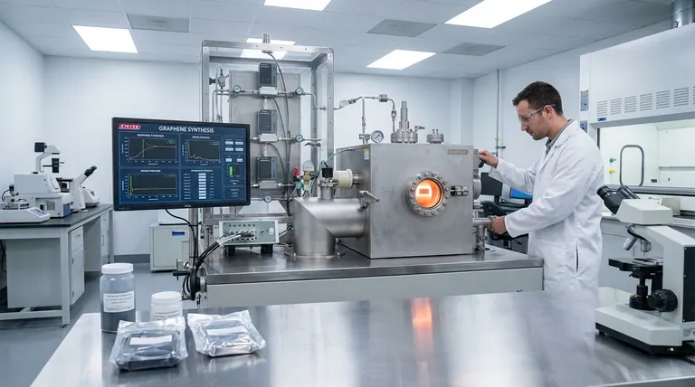
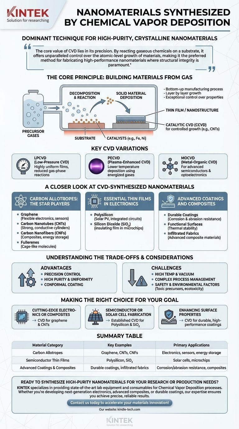
In essence, Chemical Vapor Deposition (CVD) is a dominant technique for synthesizing high-purity, crystalline nanomaterials. It is most notably used to produce a range of critical carbon-based structures, including graphene, carbon nanotubes (CNTs), and carbon nanofibers (CNFs). The method is also a cornerstone in the semiconductor industry for creating essential thin films like polysilicon and silicon dioxide.
The core value of CVD lies in its precision. By reacting gaseous chemicals on a substrate, it offers unparalleled control over the atomic-level growth of materials, making it the preferred method for fabricating high-performance nanomaterials where structural integrity is paramount.
The Core Principle: Building Materials from Gas
CVD is fundamentally a bottom-up manufacturing process. It doesn't carve material away; it builds it, layer by layer, providing exceptional control over the final product's properties.
From Gas to Solid
The process involves introducing one or more volatile precursor gases into a reaction chamber containing a heated substrate. These gases decompose and react near the substrate's surface, causing a solid material to deposit and form a thin film or nanostructure.
The Role of Catalysts
For many advanced nanomaterials, especially carbon nanotubes, catalytic CVD (CCVD) is the standard. In this variation, tiny nanoparticles of a catalyst (like iron, nickel, or cobalt) are placed on the substrate. These catalysts act as "seeds" that direct the growth of the nanotubes, offering significant control over their diameter and structure.
Key CVD Variations
The basic CVD principle can be adapted for different materials and applications. Common variations include:
- Low-Pressure CVD (LPCVD): Reduces gas-phase reactions, leading to highly uniform films.
- Plasma-Enhanced CVD (PECVD): Uses a plasma to energize the precursor gases, allowing deposition at much lower temperatures.
- Metal-Organic CVD (MOCVD): Uses metal-organic compounds as precursors, common in fabricating advanced semiconductors and optoelectronics.
A Closer Look at CVD-Synthesized Nanomaterials
While CVD can be used on a wide range of materials, it has become synonymous with the production of a few classes of high-value nanomaterials.
Carbon Allotropes: The Star Players
CVD is the leading method for synthesizing high-quality carbon nanomaterials.
- Graphene: A single atomic layer of carbon atoms, grown as large sheets via CVD for use in flexible electronics, sensors, and composites.
- Carbon Nanotubes (CNTs): Rolled sheets of graphene that form incredibly strong, conductive cylinders. CVD is favored for its structural control and cost-effectiveness.
- Carbon Nanofibers (CNFs): Similar to CNTs but with a different internal structure, often used in composites and energy storage.
- Fullerenes: Cage-like carbon molecules (like buckyballs) that can also be synthesized with specialized CVD techniques.
Essential Thin Films in Electronics
Beyond novel nanomaterials, CVD is a workhorse in mainstream technology.
- Polysilicon: A critical material used extensively in the solar photovoltaic (PV) supply chain and for manufacturing integrated circuits.
- Silicon Dioxide (SiO₂): A high-purity insulating film that is a fundamental component of virtually all modern microchips, typically deposited via LPCVD.
Advanced Coatings and Composites
The versatility of CVD allows it to enhance existing materials. It is used to apply highly durable, functional coatings on substrates like metals, ceramics, and glass to improve corrosion resistance, abrasion resistance, and thermal stability. The process can also be used to infiltrate fabrics with nanomaterials, creating advanced composite materials.
Understanding the Trade-offs and Considerations
No technique is perfect. Trustworthy evaluation requires understanding both the strengths and the limitations of Chemical Vapor Deposition.
The Advantage of Precision Control
The primary reason to choose CVD is control. It produces thin films and nanostructures with high purity and structural uniformity. Its ability to conformally coat complex, three-dimensional surfaces is a significant advantage over line-of-sight methods like physical vapor deposition (PVD).
The Challenge of Process Conditions
CVD often requires very high temperatures and vacuum conditions, which translates to high energy consumption and sophisticated, expensive equipment. Managing the flow rates of multiple precursor gases to achieve consistent results at scale can also be complex.
Environmental and Safety Factors
The precursor gases used in CVD can be toxic, flammable, or corrosive, demanding strict safety protocols. Furthermore, the synthesis process itself, particularly for nanomaterials like CNTs, has potential ecotoxicity impacts that must be managed through careful control of material consumption and emissions.
Making the Right Choice for Your Goal
Selecting a synthesis method depends entirely on the desired material and its final application.
- If your primary focus is cutting-edge electronics or composites: CVD is the industry-standard method for producing the high-quality graphene and carbon nanotubes required for these demanding applications.
- If your primary focus is semiconductor or solar cell fabrication: Established CVD processes for depositing uniform films of polysilicon and silicon dioxide are indispensable.
- If your primary focus is enhancing surface properties: CVD provides a robust solution for creating durable, high-performance coatings that can withstand extreme environments.
By understanding its principles and target materials, you can leverage CVD's precision to build the foundational components of next-generation technology.
Summary Table:
| Material Category | Key Examples | Primary Applications |
|---|---|---|
| Carbon Allotropes | Graphene, Carbon Nanotubes (CNTs), Carbon Nanofibers (CNFs) | Flexible electronics, sensors, composites, energy storage |
| Semiconductor Thin Films | Polysilicon, Silicon Dioxide (SiO₂) | Solar cells, integrated circuits, microchips |
| Advanced Coatings & Composites | Durable coatings on metals/ceramics, infiltrated fabrics | Corrosion/abrasion resistance, thermal stability, advanced composites |
Ready to synthesize high-purity nanomaterials for your research or production needs? KINTEK specializes in providing state-of-the-art lab equipment and consumables for Chemical Vapor Deposition processes. Whether you're developing next-generation electronics, advanced composites, or durable coatings, our expertise ensures you achieve precise, reliable results. Contact us today to discuss how our solutions can accelerate your materials innovation!
Visual Guide
Related Products
- Chemical Vapor Deposition CVD Equipment System Chamber Slide PECVD Tube Furnace with Liquid Gasifier PECVD Machine
- Microwave Plasma Chemical Vapor Deposition MPCVD Machine System Reactor for Lab and Diamond Growth
- 915MHz MPCVD Diamond Machine Microwave Plasma Chemical Vapor Deposition System Reactor
- Customer Made Versatile CVD Tube Furnace Chemical Vapor Deposition Chamber System Equipment
- HFCVD Machine System Equipment for Drawing Die Nano-Diamond Coating
People Also Ask
- What types of substrates are used in CVD to facilitate graphene films? Optimize Graphene Growth with the Right Catalyst
- What is plasma enhanced chemical vapor deposition PECVD equipment? A Guide to Low-Temperature Thin Film Deposition
- What happens during deposition chemistry? Building Thin Films from Gaseous Precursors
- How expensive is chemical vapor deposition? Understanding the True Cost of High-Performance Coating
- What are the core advantages of PE-CVD in OLED encapsulation? Protect Sensitive Layers with Low-Temp Film Deposition


