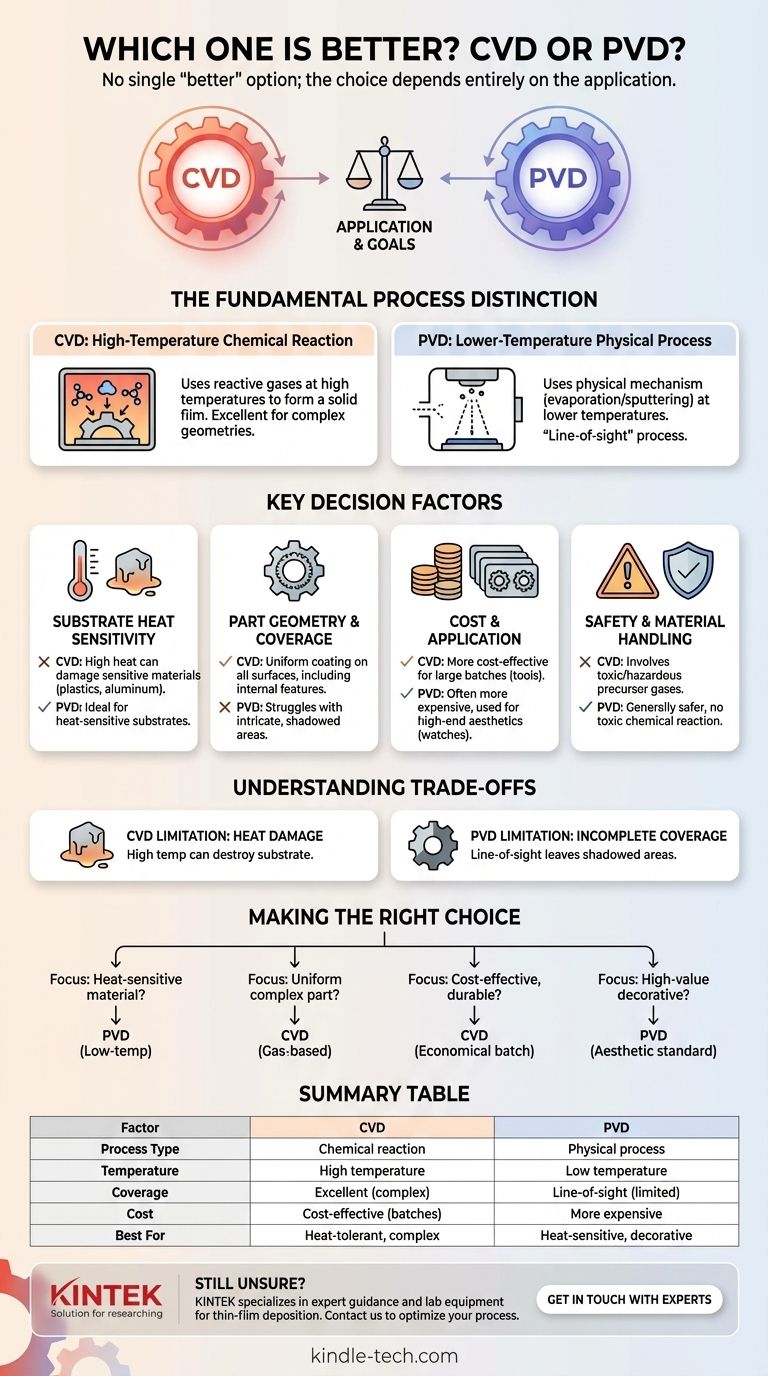
There is no single 'better' option; the choice between Chemical Vapor Deposition (CVD) and Physical Vapor Deposition (PVD) is entirely dependent on the application. The fundamental difference is that CVD uses a high-temperature chemical reaction to create a coating, while PVD uses a lower-temperature physical process. This distinction in temperature and process mechanics dictates which method is suitable for a specific substrate and desired outcome.
The choice between PVD and CVD is not about which process is superior overall, but which is compatible with your material and goals. Your decision will be driven primarily by your substrate's heat sensitivity and the complexity of the part you need to coat.
The Fundamental Process Distinction
To make an informed choice, you must first understand how each process works at a basic level. They achieve the same goal—depositing a thin film—through entirely different means.
CVD: A High-Temperature Chemical Reaction
Chemical Vapor Deposition involves introducing precursor gases into a chamber. These gases react on the surface of a heated substrate, forming a solid thin film.
The key attribute of CVD is its reliance on high temperatures to drive the chemical reaction. This process excels at creating uniform coatings that can penetrate deep holes and cover complex internal surfaces because the precursor gases can flow anywhere the substrate is exposed.
PVD: A Lower-Temperature Physical Process
Physical Vapor Deposition involves a physical mechanism, such as evaporation or sputtering, to turn a solid source material into a vapor. This vapor then travels through a vacuum and condenses onto the substrate, forming the coating.
Unlike CVD, PVD is a lower-temperature process that does not typically require heating the substrate itself. It is a "line-of-sight" process, meaning the coating material travels in a straight line from the source to the substrate.
Key Decision Factors: PVD vs. CVD
Your choice will hinge on four critical factors. Analyzing your project against these criteria will almost always reveal the correct path.
Factor 1: Substrate Heat Sensitivity
This is often the most important factor. The high temperatures required for CVD can damage or alter the properties of many materials, such as plastics, aluminum, or certain heat-treated steels.
If your substrate cannot withstand high heat, PVD is the default and often only choice.
Factor 2: Part Geometry and Coverage
CVD's use of reactive gases allows it to provide an exceptionally uniform coating on all surfaces, including complex internal geometries and deep, narrow holes.
PVD, being a line-of-sight process, struggles to coat intricate internal features effectively. For parts with complex shapes that require complete coverage, CVD holds a distinct advantage.
Factor 3: Cost and Application
Generally, CVD is the more cost-effective process. Its ability to coat many parts at once in a batch process makes it efficient for large-scale production of durable coatings on tools and other components.
PVD is typically more expensive due to its complex vacuum technology and part-handling requirements. It is often reserved for high-end products where aesthetics are critical, such as designer watches, jewelry, and premium decorative finishes.
Factor 4: Safety and Material Handling
The CVD process often involves precursor materials that can be toxic or hazardous, requiring specialized handling and safety protocols.
PVD, on the other hand, does not involve a chemical reaction with toxic byproducts, making the process inherently safer and easier to manage.
Understanding the Trade-offs
Neither technology is without its limitations. Being aware of these trade-offs is crucial for avoiding costly mistakes.
The Limitation of CVD: Heat Damage
The primary drawback of CVD is its high operating temperature. Applying it to the wrong material will result in a damaged or destroyed part, making it completely unsuitable for a wide range of common substrates.
The Limitation of PVD: Incomplete Coverage
The line-of-sight nature of PVD is its main weakness. Without complex and costly fixture rotation, it can result in uneven coating thickness or leave "shadowed" areas on complex parts completely uncoated.
The Cost-Complexity Balance
While PVD is more expensive, that cost buys you the ability to coat heat-sensitive materials. CVD is cheaper, but only if your part can tolerate the intense heat. The cost is directly tied to the physical limitations of your substrate.
Making the Right Choice for Your Application
Answering the following questions based on your project goals will lead you to the correct decision.
- If your primary focus is coating a heat-sensitive material (like plastic, aluminum, or a tempered alloy): PVD is your only viable option due to its low-temperature operation.
- If your primary focus is achieving a perfectly uniform coating on a complex part with internal channels or deep holes: CVD is the superior choice because its gas-based process ensures complete coverage.
- If your primary focus is cost-effective, durable coating for a heat-tolerant material (like carbide tooling): CVD is the more economical and efficient solution.
- If your primary focus is a high-value decorative finish on a premium product: PVD is the industry standard for its high-quality aesthetic results.
By understanding these core principles, you can confidently select the process that aligns perfectly with your material, geometry, and budget.
Summary Table:
| Factor | CVD (Chemical Vapor Deposition) | PVD (Physical Vapor Deposition) |
|---|---|---|
| Process Type | Chemical reaction | Physical process |
| Temperature | High temperature | Low temperature |
| Coverage | Excellent for complex geometries | Line-of-sight (limited coverage) |
| Cost | More cost-effective for large batches | More expensive |
| Best For | Heat-tolerant materials, complex parts | Heat-sensitive materials, decorative finishes |
Still unsure which coating process is right for your project?
At KINTEK, we specialize in providing expert guidance and high-quality lab equipment for thin-film deposition. Whether you need the uniform coverage of CVD for complex parts or the low-temperature advantages of PVD for sensitive materials, our team can help you select the perfect solution.
Contact us today for a personalized consultation and discover how KINTEK's expertise in lab equipment and consumables can optimize your coating process and improve your results.
Get in touch with our experts now!
Visual Guide
Related Products
- Inclined Rotary Plasma Enhanced Chemical Vapor Deposition PECVD Equipment Tube Furnace Machine
- HFCVD Machine System Equipment for Drawing Die Nano-Diamond Coating
- 915MHz MPCVD Diamond Machine Microwave Plasma Chemical Vapor Deposition System Reactor
- Vacuum Hot Press Furnace Machine for Lamination and Heating
- CVD Diamond Cutting Tool Blanks for Precision Machining
People Also Ask
- What is plasma enhanced chemical vapour deposition process? Unlock Low-Temperature, High-Quality Thin Films
- What is the difference between CVD and PECVD? Choose the Right Thin-Film Deposition Method
- What is the difference between PECVD and CVD? Unlock the Right Thin-Film Deposition Method
- What is PECVD silicon deposition? Achieve Low-Temperature, High-Quality Thin Films
- What materials are deposited in PECVD? Discover the Versatile Thin-Film Materials for Your Application


