Applications of Cultivated Diamonds
Use in Jewelry and Precision Tools
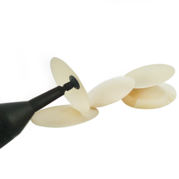
High-quality, large-size, ultra-pure CVD cultivated diamonds are not only prized for their aesthetic appeal in the jewelry industry but also for their exceptional hardness and precision in cutting tools. These diamonds, grown through advanced chemical vapor deposition (CVD) techniques, offer a level of purity and perfection that is difficult to achieve with natural diamonds.
In the realm of jewelry, these cultivated diamonds are increasingly sought after for their ethical sourcing and superior quality. They are often indistinguishable from their natural counterparts, yet they come with the added assurance of being conflict-free and environmentally friendly. This has made them a popular choice among ethically conscious consumers and high-end jewelers alike.

For precision cutting tools, the hardness and thermal conductivity of CVD cultivated diamonds make them indispensable. They are used in a variety of applications, from surgical instruments to micro-drills and saws, where precision and durability are paramount. The ability to grow these diamonds in controlled environments allows for the production of uniform, high-quality tools that can withstand extreme conditions and maintain their sharpness over extended periods.
Moreover, the versatility of CVD cultivated diamonds extends beyond their current applications. Ongoing research and development are exploring new ways to leverage their unique properties, potentially expanding their use into even more demanding industries. This continuous innovation ensures that CVD cultivated diamonds will remain at the forefront of both luxury and precision technology.
Use in High-End Advanced Manufacturing
Cultivated diamonds have emerged as a critical component in high-end advanced manufacturing, particularly in sectors that demand exceptional material properties. These synthetic gems are employed in various high-tech applications, including optical windows, where their transparency and hardness ensure optimal performance in high-stress environments. In the realm of semiconductors, cultivated diamonds play a pivotal role in heat sinking, effectively managing the thermal loads generated by high-performance chips. This capability is crucial for maintaining the integrity and longevity of electronic devices.
Moreover, the use of cultivated diamonds in power devices underscores their versatility and robustness. These diamonds are integral to the development of efficient power converters and switches, enhancing the overall performance and reliability of power systems. The unique combination of thermal conductivity, electrical insulation, and mechanical strength makes cultivated diamonds an indispensable material in the ongoing evolution of advanced manufacturing technologies.
Technological Advancements in Diamond Cultivation
MPCVD Technology
Microwave plasma chemical vapor deposition (MPCVD) is a sophisticated chemical vapor deposition process that leverages a continuous microwave source to generate and sustain a highly reactive plasma. This plasma comprises the reacting chemicals and essential catalysts, facilitating the deposition of layers of diamond onto a diamond-seeded substrate. The process involves introducing methane and hydrogen gases, which interact with the plasma to grow new diamond structures.
One of the standout features of MPCVD technology is its ability to introduce dopants into the carbon structure during the growth process. For instance, the addition of boron can create superconducting diamond, while nitrogen vacancies can produce intriguing photo-luminescence properties. These characteristics are particularly valuable in quantum information systems, where precise control over material properties is paramount.
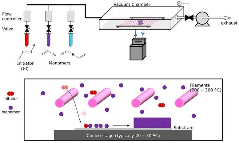
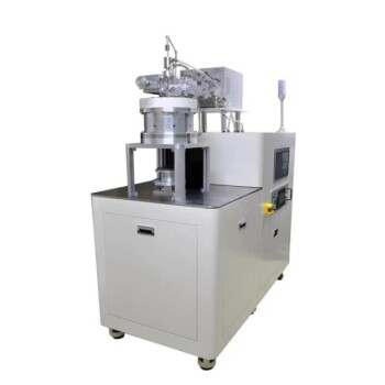
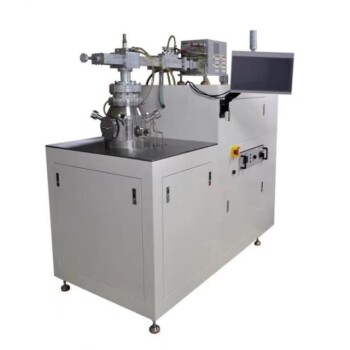
The MPCVD system itself is a complex apparatus consisting of a vacuum chamber, a microwave generator, and a gas delivery system. The microwave generator plays a crucial role in creating a plasma within the vacuum chamber, which then decomposes and deposits gas species onto the substrate. This meticulous process ensures the production of large-size, high-purity cultivated diamonds, making MPCVD a cornerstone technology in the field of diamond synthesis.
CVD Synthesis and Wafer Splicing
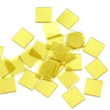
Chemical Vapor Deposition (CVD) synthesis is a groundbreaking technique in the production of high-purity, plate-like diamonds. This method excels in creating diamonds that are not only of exceptional quality but also suitable for large-area single-crystal wafers. The process involves the careful manipulation of gas mixtures under precise conditions, resulting in the deposition of carbon atoms onto a substrate, which gradually forms a diamond layer.
One of the key advantages of CVD synthesis is its ability to produce diamonds with minimal impurities, ensuring a high degree of purity that is crucial for semiconductor applications. These diamonds are often characterized by their uniform crystal structure, which is essential for maintaining consistency across large wafer surfaces.
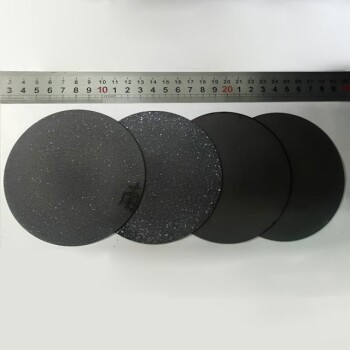
The application of CVD-synthesized diamonds in wafer splicing is particularly noteworthy. Wafer splicing involves joining multiple diamond wafers to create a continuous, larger surface area, which is vital for enhancing the efficiency and performance of semiconductor devices. The high purity and uniform structure of CVD diamonds make them ideal for this process, as they minimize defects and ensure seamless integration.
In summary, CVD synthesis not only enables the production of high-purity, plate-like diamonds but also facilitates their effective use in wafer splicing, thereby contributing significantly to advancements in semiconductor technology.
Challenges and Solutions in Semiconductor Heat Dissipation
Heat Dissipation Issues in 5G and New Energy Vehicles
The rapid advancement of 5G technology and the proliferation of new energy vehicles have created a pressing need for efficient heat dissipation solutions. As these technologies operate at higher frequencies and power levels, the heat generated can significantly impact performance and longevity. Traditional cooling methods often fall short in managing the intense heat loads produced by these systems.
For instance, 5G base stations and new energy vehicle batteries generate substantial heat during operation. This heat must be effectively managed to prevent overheating, which can lead to performance degradation, system failures, and safety hazards. The challenge is compounded by the compact and densely packed components typical of these advanced systems, which limit the available space for conventional cooling solutions.
To address these challenges, innovative heat dissipation technologies are being developed. One promising approach involves the use of cultivated diamonds, known for their exceptional thermal conductivity. These diamonds can serve as effective heat sinks, efficiently transferring heat away from critical components. Additionally, new encapsulation substrates with high thermal conductivity are being researched to provide lightweight and efficient cooling solutions.
In summary, the integration of advanced materials like cultivated diamonds and the development of new encapsulation substrates are crucial steps towards resolving the heat dissipation issues in 5G and new energy vehicles. These innovations not only enhance system performance but also ensure the reliability and safety of these cutting-edge technologies.
Development of New Encapsulation Substrates
The rapid advancement of semiconductor technology, particularly in the realms of 5G and new energy vehicles, necessitates the development of innovative encapsulation substrates that can effectively manage heat dissipation. Traditional materials often fall short in meeting the stringent requirements of modern electronic devices, which demand not only high thermal conductivity but also lightweight properties to ensure optimal performance and durability.
To address these challenges, researchers are focusing on the development of new lightweight electronic packaging materials that boast exceptional thermal conductivity. These materials are engineered to provide a superior balance between thermal management and structural integrity, crucial for the efficient operation of high-performance devices. The integration of such advanced substrates into electronic systems promises to enhance overall system reliability and longevity, while also enabling the miniaturization of components without compromising on performance.
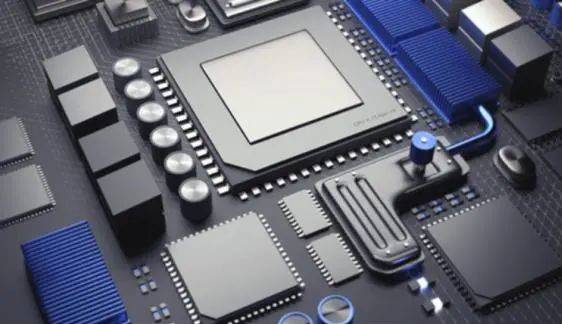
The pursuit of these new encapsulation substrates is not just a response to current technological demands but also a proactive step towards future innovations in semiconductor and high-end manufacturing sectors. By leveraging cutting-edge materials science and engineering techniques, the industry is poised to overcome existing limitations and pave the way for next-generation electronic devices that are both powerful and sustainable.
In summary, the development of new encapsulation substrates with high thermal conductivity and lightweight characteristics is a critical area of focus that holds significant promise for the future of semiconductor technology and advanced manufacturing.
Future Prospects of Cultivated Diamonds
Potential in Semiconductor Industry
Cultivated diamonds are increasingly being recognized as the ultimate semiconductor material, primarily due to their exceptional thermal conductivity. This property is crucial in the semiconductor industry, where efficient heat dissipation is essential to maintain optimal device performance and longevity. Unlike traditional materials, cultivated diamonds can handle higher temperatures without degrading, making them ideal for the high-stress environments found in advanced semiconductor applications.
Moreover, cultivated diamonds offer additional benefits that further enhance their suitability for semiconductor use. Their chemical inertness ensures stability under various operating conditions, while their high electron mobility supports faster data processing and transmission. These characteristics make cultivated diamonds not just a superior thermal conductor but also a versatile material for enhancing the overall efficiency and reliability of semiconductor devices.
In the context of emerging technologies like 5G and new energy vehicles, the need for advanced heat dissipation solutions is more critical than ever. Cultivated diamonds' superior thermal management capabilities position them as a key component in the development of next-generation semiconductors, promising to drive innovation and performance in these rapidly evolving fields.
Research and Development Trends
Major manufacturers are increasingly focusing their R&D efforts on the development of high thermal conductivity substrate materials. This strategic investment is driven by the growing demand for efficient heat dissipation solutions, particularly in the semiconductor industry, where heat management is critical for optimal performance and longevity of devices.
The semiconductor industry, in particular, is witnessing a surge in the use of cultivated diamonds due to their exceptional thermal conductivity properties. These diamonds are not only being explored for their potential in traditional semiconductor applications but also in emerging technologies such as 5G and new energy vehicles. The high thermal conductivity of cultivated diamonds ensures that they can effectively manage the heat generated by these high-performance devices, thereby enhancing their operational efficiency and lifespan.
Moreover, advancements in Microwave Plasma Chemical Vapor Deposition (MPCVD) technology and CVD synthesis are enabling the production of large-size, high-purity cultivated diamonds. These technological breakthroughs are paving the way for the development of new encapsulation substrates that are both lightweight and possess superior thermal conductivity. Such materials are essential for the next generation of electronic packaging, where thermal management is a key consideration.
In summary, the ongoing R&D efforts in high thermal conductivity substrate materials are not only addressing the immediate needs of the semiconductor industry but also laying the groundwork for future technological advancements.
Related Products
- Microwave Plasma Chemical Vapor Deposition MPCVD Machine System Reactor for Lab and Diamond Growth
- CVD Diamond for Thermal Management Applications
- Cylindrical Resonator MPCVD Machine System Reactor for Microwave Plasma Chemical Vapor Deposition and Lab Diamond Growth
- CVD Diamond Domes for Industrial and Scientific Applications
- Laboratory CVD Boron Doped Diamond Materials
Related Articles
- The Advancements in MPCVD Systems for Large Size Single Crystal Diamonds
- Understanding MPCVD: A Comprehensive Guide to Microwave Plasma Chemical Vapor Deposition
- Comparing Chemical Vapor Deposition and Physical Vapor Deposition
- Advantages, Limitations, and Process Control of Chemical Vapor Deposition (CVD) Technology
- The Process of Fabricating a CVD Diamond By MPCVD Machine
