Overview of Diamond Optical Window Components
Introduction to Diamond as a Material
Diamond, often celebrated for its brilliance in jewelry, is also a third-generation ultra-wideband semiconductor material with a face-centered cubic structure. This unique crystalline form endows diamond with an array of exceptional properties that make it highly suitable for a variety of advanced technological applications.
One of the most remarkable aspects of diamond is its mechanical robustness. It boasts the highest hardness and wear resistance among all known materials, which ensures durability in high-stress environments. This mechanical strength is complemented by its outstanding thermal conductivity, which is superior to that of copper and silver, making diamond an excellent choice for components that require efficient heat dissipation.
In the realm of optics, diamond's transparency extends across a broad spectrum, from ultraviolet to infrared light. This optical versatility is crucial for applications in high-energy laser systems, infrared sensors, and even X-ray windows. Furthermore, diamond's electrical properties are equally impressive; it exhibits a high breakdown voltage and low dielectric constant, making it ideal for use in high-power electronic devices.
The combination of these properties—mechanical, thermal, optical, and electrical—positions diamond as a material of choice for cutting-edge technologies in defense, aerospace, and energy sectors. Its ability to perform reliably under extreme conditions underscores its potential to revolutionize various industries, making it a cornerstone in the development of next-generation optical window components.
Synthesis Methods for Diamond Optical Components
Diamond optical window components are meticulously crafted through advanced synthesis techniques, primarily utilizing methods such as microwave plasma chemical vapor deposition (MPCVD), hot wire chemical vapor deposition (HWCVD), and DC arc plasma jet injection chemical vapor deposition (DCAPCVD). These techniques enable the creation of high-quality diamond thin films, which are essential for applications ranging from radiation sensing to high-power laser windows.
Given the scarcity and high demand for natural diamond in desired quality and quantity, extensive research has focused on synthesizing diamond in laboratory settings. Notably, the properties of laboratory-synthesized diamonds are nearly identical to those of naturally occurring single crystal diamonds, making them a viable alternative. The choice of synthesis method often depends on the specific application and the desired properties of the diamond film.
For instance, chemical vapor deposition (CVD) methods are particularly favored for producing synthetic polycrystalline diamond windows, which are shaped as disks with large diameters and small thicknesses to minimize absorption. These windows are increasingly replacing traditional materials like zinc selenide in high-power CO2 lasers and gyrotrons. Additionally, recent advancements in high-pressure high-temperature (HPHT) and CVD techniques have significantly improved the purity and crystallographic structure of single-crystalline diamond, making it suitable for applications such as diffraction gratings and window materials in high-power radiation sources.
Moreover, these synthesis methods are not limited to optical applications. They are also employed to create designer optically transparent diamond anvils, which are crucial for measuring the electric and magnetic properties of materials at ultra-high pressures using a diamond anvil cell. This versatility underscores the importance of synthetic diamond in both current and emerging technologies.
Applications of Diamond Optical Window Components
Infrared Band Applications
Diamond optical windows play a pivotal role in infrared (IR) applications, particularly in airborne, ballistic, and shipboard systems. These windows are integral to infrared search and tracking systems, which are crucial for early detection and tracking of targets in various military and surveillance contexts. The exceptional thermal conductivity and transmittance of diamond make it an ideal material for these applications, ensuring that the systems operate efficiently even under extreme conditions.
In addition to their use in search and tracking systems, diamond optical windows are also employed in high-energy laser weapon systems. The high damage threshold and optical clarity of diamond windows ensure that they can withstand the intense energy levels required for laser operations, making them indispensable in modern defense technology.
Furthermore, the versatility of diamond optical windows extends beyond military applications. They are also utilized in civil and commercial sectors, such as in advanced imaging and spectroscopy systems. The broad spectral range of diamond, from the visible to the far-infrared, makes it a preferred choice for these applications, enabling precise and detailed analysis of various materials and environments.
| Application Area | Key Benefits of Diamond Optical Windows |
|---|---|
| Infrared Search and Tracking | High thermal conductivity, excellent transmittance |
| High-Energy Laser Weapons | High damage threshold, optical clarity |
| Advanced Imaging and Spectroscopy | Broad spectral range, precise analysis capabilities |
The unique properties of diamond optical windows, such as their high thermal conductivity, optical clarity, and broad spectral range, make them indispensable in a variety of infrared applications, ensuring superior performance and reliability in both military and civilian contexts.
Microwave and Terahertz Band Applications
Diamond components play a pivotal role in the development of high-power microwave weapons and terahertz traveling wave tubes. These components are indispensable due to their exceptional transmittance and mechanical strength, which are critical for the performance of these advanced systems.
In the realm of microwave weapons, diamond's high transmittance ensures that the electromagnetic waves can propagate without significant loss, thereby maintaining the weapon's effectiveness. Similarly, in terahertz traveling wave tubes, the mechanical strength of diamond allows for the construction of robust components that can withstand the high-stress environments associated with these devices.
Moreover, the unique properties of diamond make it an ideal material for both high-power microwave and terahertz applications. Its ability to transmit electromagnetic waves efficiently, coupled with its mechanical durability, positions diamond as a superior choice over other materials in these cutting-edge technologies.
| Application Area | Key Benefits of Diamond Components |
|---|---|
| High-Power Microwave Weapons | High transmittance, Mechanical strength |
| Terahertz Traveling Wave Tubes | High transmittance, Mechanical strength |
The integration of diamond components in these applications not only enhances the performance but also opens up new possibilities for innovation in defense and aerospace sectors. As research and development continue, the role of diamond in these high-tech fields is expected to grow, further solidifying its status as a material of choice for advanced optical window components.
X-ray and Extreme Ultraviolet Applications
Diamond films are not just used in X-ray windows but also play a pivotal role in extreme ultraviolet (EUV) lithography systems. The exceptional transmittance of diamond films in these high-energy spectra, combined with their superior mechanical properties, makes them indispensable in advanced imaging technologies.
In X-ray applications, diamond windows are favored for their ability to withstand high pressures and temperatures while maintaining high transmittance. This makes them ideal for use in synchrotron radiation sources and X-ray telescopes, where the integrity of the window material is crucial for accurate data collection.
For EUV lithography, diamond films serve as core components in the optical systems that are essential for the production of microchips with nanometer-scale features. The high transmittance of diamond in the EUV range allows for precise imaging, while its mechanical strength ensures the longevity and reliability of the lithography equipment.
| Application | Material Property Utilized | Key Benefit |
|---|---|---|
| X-ray Windows | High transmittance, mechanical strength | Accurate data collection, durability under high pressure |
| EUV Lithography | High transmittance, mechanical strength | Precise imaging, equipment longevity |
The unique combination of optical and mechanical properties in diamond makes it the material of choice for these demanding applications, pushing the boundaries of what is possible in both scientific research and industrial production.
Preparation and Processing of Diamond Optical Elements
Curved Surface Processing
The development of techniques for preparing large-area, high-quality curved diamond films is crucial for applications requiring conformal structures. These techniques are essential for creating optical components that can conform to complex geometries, thereby enhancing their performance in various fields such as defense, aerospace, and energy.
One of the primary challenges in this area is ensuring that the diamond films maintain their exceptional mechanical, thermal, and optical properties while being shaped into curved surfaces. This requires advanced processing methods that can handle the unique characteristics of diamond, such as its hardness and thermal conductivity.
| Processing Technique | Key Features | Applications |
|---|---|---|
| Laser Cutting | Precision cutting with minimal heat-affected zone | Aerospace components, high-precision optical windows |
| Ion Beam Machining | Non-contact, high-precision surface modification | Defense optics, conformal infrared sensors |
| Chemical Etching | Controlled removal of material using chemical reactions | Energy sector components, curved X-ray windows |
These techniques not only enable the fabrication of curved diamond films but also ensure that the resulting components meet the stringent requirements for high transmittance, mechanical strength, and thermal stability needed in advanced optical systems. By mastering these processes, researchers can push the boundaries of what is possible with diamond optical components, opening up new possibilities in high-tech applications.
Surface Polishing Processes
Achieving the perfect surface finish for diamond optical elements is a complex process that involves a variety of advanced techniques. These methods can be broadly categorized into mechanical, chemo-mechanical, thermochemical, and other specialized processes such as dynamic friction, laser, ion beam, plasma etch, and electrical discharge machining (EDM). Each of these techniques has its unique advantages and applications, tailored to meet the stringent requirements of diamond optical components.
Mechanical Polishing is one of the most traditional methods, relying on abrasive materials to gradually remove surface imperfections. This technique is particularly effective for achieving a smooth finish on flat surfaces. However, it can be time-consuming and may require multiple stages of polishing to reach the desired level of smoothness.
Chemo-Mechanical Polishing combines chemical reactions with mechanical abrasion, allowing for more precise control over the polishing process. This method is particularly useful for delicate surfaces where traditional mechanical polishing might cause damage.
Thermochemical Polishing leverages heat to induce chemical reactions that alter the surface of the diamond. This technique is highly effective for removing deep-seated imperfections and can be used in conjunction with other methods to achieve a superior finish.
In addition to these primary methods, specialized techniques such as dynamic friction polishing, laser polishing, ion beam polishing, plasma etching, and EDM offer unique capabilities. Dynamic friction polishing, for example, uses high-speed rotation and friction to smooth surfaces, while laser polishing employs laser beams to remove material in a highly controlled manner. Ion beam polishing uses accelerated ions to etch the surface, providing a very fine and controlled finish. Plasma etching, on the other hand, uses plasma to remove material, offering a high degree of precision. Finally, EDM, or electrical discharge machining, uses electrical discharges to erode material, making it ideal for intricate shapes and hard-to-reach areas.
Each of these methods plays a crucial role in the fabrication of diamond optical elements, ensuring that they meet the high standards required for their intended applications in various fields, including defense, aerospace, and energy.
Conclusion and Future Directions
Summary of Diamond Optical Window Advantages
Diamond optical window elements harness the exceptional properties of diamond to excel in a multitude of high-tech applications, particularly in defense and energy sectors. Diamond's unparalleled hardness, chemical inertness, high thermal conductivity, and low coefficient of thermal expansion make it the superior choice over any other existing window material for transmitting infrared and microwave radiation. This superiority is evident in its increasing use as the output window for high-power CO2 lasers and gyrotrons, replacing traditional materials like zinc selenide.
Synthetic polycrystalline diamond windows, produced via the Chemical Vapor Deposition (CVD) technique, are shaped into disks with large diameters and minimal thickness to reduce absorption, making them ideal for high-power applications. Additionally, single-crystal diamond slabs, with dimensions reaching up to approximately 10 mm, are becoming pivotal in various optical fields, including heatspreaders within laser cavities, diffractive optics, and as the gain medium in Raman lasers.
Recent advancements in High-Pressure High-Temperature (HPHT) and CVD synthesis techniques have significantly enhanced the purity and crystallographic perfection of single-crystalline diamond, enabling its use as a diffraction grating and window material in high-power radiation sources such as synchrotrons. Both CVD and HPHT processes are also employed to create optically transparent diamond anvils, essential tools for measuring the electric and magnetic properties of materials under ultra-high pressures using a diamond anvil cell.
The optical applications of CVD diamond are broadly categorized into self-supported film windows, optical crystals, and optical coatings. These applications span across all wavelength bands, from X-ray to microwave, making diamond windows indispensable in microwave systems, missile windows/fairings, X-ray windows, laser windows, microlenses, and other components in nuclear fusion, airborne, bomb, shipborne, and space-based systems.
Diamond's unique properties, such as its high atomic density and strong bonding, coupled with its highly symmetric lattice structure, result in significant Raman gain, as illustrated in Table 3. Furthermore, its high refractive index and acoustic transmission velocity contribute to a high Brillouin gain and frequency shift, as shown in Table 4. These characteristics position diamond crystals as the ideal medium for high-power and high-efficiency Raman and Brillouin laser operations.
In summary, diamond optical windows are revolutionizing high-tech applications due to their superior properties, making them indispensable in defense, energy, and numerous other sectors.
Challenges and Research Needs
The demand for large-size optical-grade diamond preparation and precision processing remains a significant challenge, particularly in high power, high temperature, and high frequency applications. These applications require not only the synthesis of large, flawless diamonds but also their precise shaping and polishing to meet the stringent requirements of optical clarity and mechanical strength.
Currently, the methods for preparing diamond optical components, such as microwave plasma chemical vapor deposition and hot wire chemical vapor deposition, face limitations in scaling up to produce large-size diamonds. Additionally, the surface polishing processes, which include techniques like mechanical, chemo-mechanical, and laser polishing, must be refined to ensure that the diamond surfaces remain free from defects that could compromise their optical properties.
Moreover, the need for conformal structures in certain applications, such as curved surface processing, adds another layer of complexity. Developing techniques that can efficiently produce large-area, high-quality curved diamond films is essential but remains an area where significant advancements are needed.
In summary, while diamond optical window components offer unparalleled advantages in various high-tech fields, their preparation and processing must undergo substantial improvements to fully meet the demands of modern applications.
Related Products
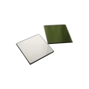
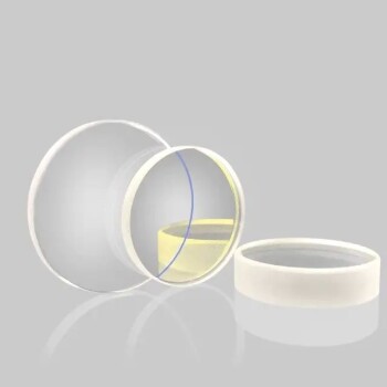
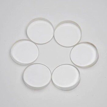
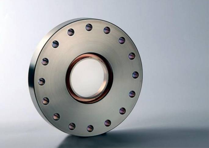
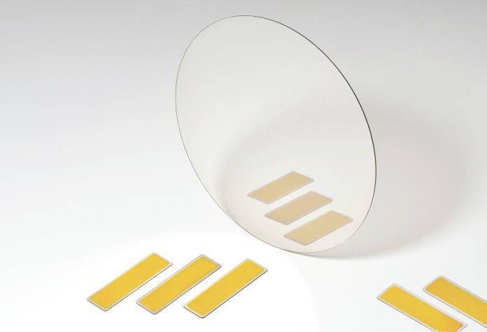
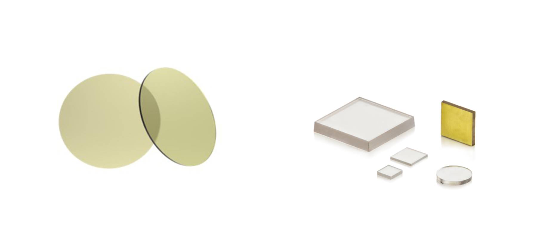
- CVD Diamond Optical Windows for Lab Applications
- MgF2 Magnesium Fluoride Crystal Substrate Window for Optical Applications
- Optical Window Glass Substrate Wafer Quartz Plate JGS1 JGS2 JGS3
- Optical Window Glass Substrate Wafer Single Double Sided Coated K9 Quartz Sheet
- Infrared Transmission Coating Sapphire Sheet Substrate Window
Related Articles
- Chemical Vapor Deposition (CVD) of Graphene Challenges and Solutions
- Advantages and Disadvantages of Chemical Vapor Deposition (CVD)
- Market Prospects and Applications of CVD Diamonds
- CVD Machines for Thin Film Deposition
- Comprehensive Guide to Optical Windows: Material Properties and Surface Specifications