Introduction to Sputtering Deposition
Definition and Advantages
Sputtering coating is a sophisticated technology that involves bombarding the target surface with energetic particles within a vacuum chamber. This bombardment results in the ejection of atoms and other particles from the target, which are then deposited onto a substrate to form a thin film. The process relies on the transfer of momentum from the energetic particles to the target atoms, leading to their displacement and subsequent deposition on the substrate.
One of the key advantages of sputtering coating is its ability to achieve large-area rapid deposition. This capability is crucial for applications requiring extensive coverage, such as in the manufacturing of optical coatings or semiconductor devices. Additionally, the films produced through sputtering exhibit excellent bonding with the substrate, ensuring durability and longevity.
Another significant advantage is the high sputtering density achieved, which translates to fewer pinholes in the deposited film. Pinholes can compromise the integrity and performance of the film, making their reduction a critical factor in the quality of the final product. The controllability and repeatability of the sputtering process are also noteworthy, allowing for precise adjustments and consistent results across multiple runs.
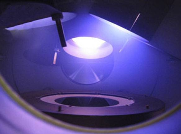
Sputtering technology is highly versatile, capable of depositing films from virtually any material, including metals, alloys, and even complex compounds. This flexibility opens up a wide range of applications, from the creation of functional coatings in electronics to the development of protective layers in aerospace engineering. The ability to sputter any material ensures that the technology can be tailored to meet specific requirements, making it a powerful tool in various industries.
Mechanisms of Sputtering
Cascade Collision and Sputtering
When incident ions strike the target surface, they transfer a portion of their energy to the surface lattice atoms, initiating a complex series of atomic movements. This energy transfer can displace atoms from their lattice positions, some of which gain enough energy to overcome the surface potential barrier and sputter directly. Others, however, remain constrained within the lattice, causing them to vibrate in place and raise the local temperature of the target material.
A significant number of atoms, upon receiving sufficient energy, undergo a recoil event. These recoiled atoms collide with neighboring atoms, displacing them and setting off a chain reaction of higher-order recoils. This cascading series of collisions is termed a cascade collision. During this process, if the energy of the cascade reaches the surface and exceeds the surface binding energy, atoms can be ejected from the material, a phenomenon known as cascade sputtering.
The process can be visualized as a linear collision cascade, where the incoming ion (purple circle) initiates a series of recoils (red, blue, green, and yellow circles) that eventually lead to atoms being ejected from the target. If the target is thin, these ejected atoms can escape from the back side, a process referred to as "sputtering in transmission."
In essence, cascade collision and sputtering are fundamental mechanisms that drive the atom displacement and ejection necessary for the formation of thin films in sputtering deposition technology.
Types of Sputtering Techniques
Diode Sputtering
Diode sputtering represents the foundational and most elementary form of sputtering technology. This method involves a straightforward setup comprising a cathode and an anode within a low-pressure vacuum chamber. The target material, typically a conductive film, serves as the cathode, while the anode accommodates the substrate to be coated. When the electric field within the chamber intensifies to a critical threshold, an anomalous glow discharge is initiated, creating a plasma environment between the two electrodes.
In this plasma state, free electrons are accelerated towards the anode, colliding with neutral gas atoms, such as Argon. These collisions ionize the gas atoms, transforming them into positively charged ions. These ions, under the influence of the electric field, accelerate towards the cathode, bombarding the target material. This bombardment results in the ejection of target atoms, a process known as sputtering. These ejected atoms then travel through the plasma and condense onto the substrate, forming a thin film.
The diode sputtering process is characterized by its simplicity and early adoption, though it is not without its challenges. One notable limitation is the relatively low deposition rate, which can lead to extended coating times and potential overheating of the target material. This issue can compromise the atomic integrity of the target, necessitating advancements such as magnetron sputtering to address these inefficiencies. Despite its limitations, diode sputtering remains a critical baseline in understanding more complex sputtering techniques.
Triode Sputtering
While diode sputtering offers simplicity, it suffers from unstable discharges and low deposition rates. To address these limitations, the triode sputtering method introduces a hot cathode into the diode sputtering setup, transforming it into a triode configuration. This modification significantly enhances the control over the sputtering process.
In triode sputtering, the plasma density can be meticulously regulated by adjusting the electron emission current and acceleration voltage. This fine-tuning capability allows for more precise control over the ionization process within the chamber. Additionally, the bombardment energy of ions on the target material can be modulated by varying the target voltage. This strategic control resolves the inherent conflicts between target voltage, target current, and gas pressure, which are common challenges in diode sputtering.
| Parameter | Control Mechanism | Impact |
|---|---|---|
| Electron Emission Current | Adjusts plasma density | Enhances ionization control |
| Acceleration Voltage | Modulates plasma density | Optimizes ionization process |
| Target Voltage | Regulates ion bombardment energy | Improves target material sputtering |
The introduction of a hot cathode in triode sputtering not only boosts the deposition rate but also enhances the overall quality of the deposited film. This method is particularly advantageous for applications requiring high-quality, uniform films with improved controllability and repeatability.
Magnetron Sputtering
Magnetron sputtering, often referred to as high-speed low-temperature sputtering, is a sophisticated plasma-based coating technique. This method leverages the interaction between a magnetically confined plasma and a negatively charged target material. When positively charged energetic ions from the plasma collide with the target, they eject atoms through a process known as "sputtering." These ejected atoms then travel through the plasma and deposit onto a substrate, forming a thin film.
The process occurs within a closed magnetic field, which serves to trap electrons and enhance the efficiency of the sputtering. By operating at lower pressures, magnetron sputtering minimizes gas incorporation in the film and reduces energy losses in the sputtered atoms. This results in high-quality films with exceptional scalability, making it a preferred method over other physical vapor deposition (PVD) techniques.
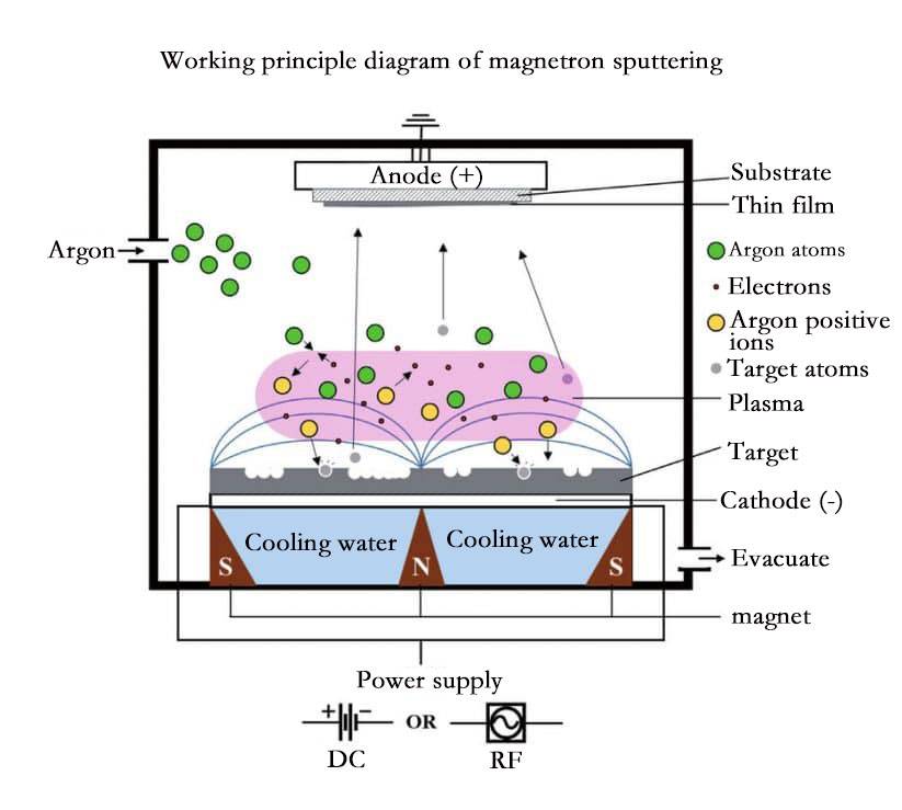
One of the key advantages of magnetron sputtering is its high deposition rate, which significantly reduces the substrate temperature rise. This is particularly beneficial for maintaining the integrity of temperature-sensitive substrates. Additionally, the method offers excellent film quality, repeatability, and ease of industrialization, making it a versatile and reliable choice for various applications.
Compared to dipole sputtering, magnetron sputtering stands out due to its superior performance in terms of deposition rate, film quality, and overall process efficiency. The combination of electric and magnetic fields near the target creates an E×B drift, which bends and prolongs the electrons' flight paths. This results in a high degree of gas ionization and a relatively high-density plasma. Ions accelerated towards the cathode/target sputter out the material, which then forms a thin film on the substrate located above the target.
In summary, magnetron sputtering's ability to produce high-quality films with minimal substrate temperature rise and its scalability make it a superior choice for industrial applications and research alike.
Reactive Magnetron Sputtering
Reactive magnetron sputtering involves the use of a metal, alloy, low-valent metal compound, or semiconductor material as the target cathode. During the sputtering process, this target material reacts with gas particles introduced into the vacuum chamber, leading to the formation of a compound film either during the sputtering process itself or as the material deposits onto the substrate surface. This method is particularly notable for its ability to produce high-purity compound films with precise control over film properties.
The process leverages the plasma environment within the vacuum chamber, where gases like nitrogen or oxygen, which are ordinarily stable and inert, become ionized and highly reactive due to high-energy collisions. These reactive gas particles then interact with the target material, facilitating the creation of complex compound structures.
One of the key advantages of reactive magnetron sputtering is its efficacy in handling large-area, uniform thin films. This capability makes it a preferred technique for the mass production of compound films, where consistency and high purity are critical. The method’s ability to control film properties ensures that the resulting coatings meet stringent specifications, making it a versatile and reliable choice for various industrial applications.
Unbalanced Magnetron Sputtering
Unbalanced magnetron sputtering employs a unique magnetic field configuration that diverges from the traditional, balanced setup. This "leaky" magnetic field design allows some of the magnetic field lines to extend beyond the target, reaching the substrate. This extension facilitates the movement of secondary electrons, which in turn enhances the plasma's reach towards the substrate. The result is a significant increase in ion currents flowing to the substrate, which can be up to ten times higher than those achievable with conventional magnetron sputtering.
The key advantage of this technique lies in its ability to not only deposit particles to form thin films but also to bombard the substrate with plasma. This dual action significantly enhances the film quality by restructuring the coating at the atomic level. The low-energy ions, which are ideal for this restructuring process, ensure that the deposited films possess optimal properties.
However, unbalanced magnetron sputtering is not without its challenges. The increased ion bombardment can lead to higher substrate heating, sometimes reaching temperatures of up to 250°C, and can introduce structural defects. Despite these limitations, the technology remains highly valuable for the preparation of various hard films, where the trade-offs are acceptable for the enhanced film properties it delivers.
Related Products
- Chemical Vapor Deposition CVD Equipment System Chamber Slide PECVD Tube Furnace with Liquid Gasifier PECVD Machine
- Customer Made Versatile CVD Tube Furnace Chemical Vapor Deposition Chamber System Equipment
- HFCVD Machine System Equipment for Drawing Die Nano-Diamond Coating
- RF PECVD System Radio Frequency Plasma-Enhanced Chemical Vapor Deposition RF PECVD
- 915MHz MPCVD Diamond Machine Microwave Plasma Chemical Vapor Deposition System Reactor
Related Articles
- In-Depth Examination of Chemical Vapor Deposition (CVD) Coatings
- Advantages, Limitations, and Process Control of Chemical Vapor Deposition (CVD) Technology
- A Comprehensive Guide to PECVD Equipment Maintenance
- Detailed Processes and Parameters of PECVD for TiN and Si3N4 Deposition
- Comprehensive Overview of 12 Types of Chemical Vapor Deposition (CVD) Techniques

