All Questions
What Does An E-Beam Do? A Versatile Tool For Welding, Sterilization, And Microfabrication
Discover how electron beams (e-beams) work and their key applications in welding, sterilization, additive manufacturing, and semiconductor lithography.
What Is The Difference Between Sputtering And E-Beam? Choose The Right Thin Film Deposition Method
Learn the key differences between sputtering and e-beam evaporation PVD methods for thin film deposition, including adhesion, purity, and material compatibility.
How Does E-Beam Deposition Work? A Guide To High-Purity Thin Film Coating
Learn how electron-beam deposition creates pure, high-quality thin films for optics and electronics. Understand the process, advantages, and limitations.
How Does Electron Beam Curing Work? Achieve Instant, Durable Curing For Industrial Applications
Discover how electron beam curing uses high-energy electrons to instantly solidify inks, coatings, and adhesives with superior durability and no VOCs.
What Materials Are Used In E-Beam Evaporation? From Pure Metals To High-Temp Ceramics
Explore the wide range of e-beam evaporation materials, including high-melting-point metals, precious metals, and dielectric ceramics for advanced coatings.
What Is The Electron Beam Method? A Guide To Precision Coating, Cutting & Sterilization
Learn how electron beam technology uses a focused stream of electrons in a vacuum for precise coating, machining, and sterilization applications.
What Is Electron Beam Coating? A Guide To High-Performance Pvd Thin Films
Discover electron beam coating, a PVD process for durable, thin films. Learn its advantages over CVD and how to choose the right method for your application.
Related Products
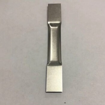
Molybdenum Tungsten Tantalum Evaporation Boat for High Temperature Applications

Evaporation Boat for Organic Matter
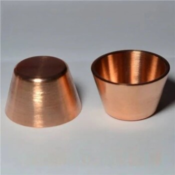
Electron Beam Evaporation Coating Oxygen-Free Copper Crucible and Evaporation Boat
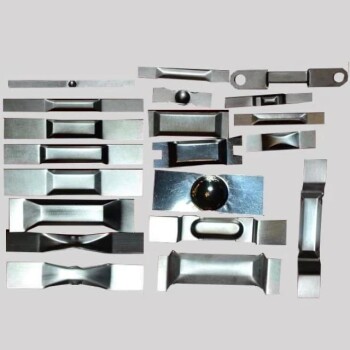
Molybdenum Tungsten Tantalum Special Shape Evaporation Boat
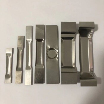
Tungsten Evaporation Boat for Thin Film Deposition