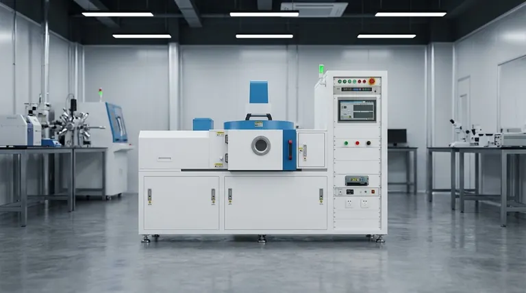
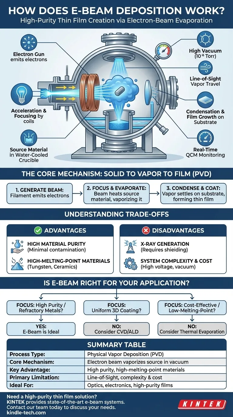
At its core, electron-beam deposition is a high-vacuum process that uses a focused, high-energy beam of electrons to heat and vaporize a source material. This vapor then travels through the vacuum and condenses onto a substrate, forming a very pure, high-quality thin film. It is a highly controlled method for creating coatings for optics, electronics, and advanced materials.
The central principle of e-beam deposition is precision energy transfer. Unlike methods that heat an entire container, the electron beam directly heats only the source material, ensuring high purity and the ability to evaporate materials with extremely high melting points.
The Core Mechanism: From Solid to Vapor
E-beam deposition is a type of Physical Vapor Deposition (PVD), meaning the material transitions from a solid to a vapor and back to a solid without a chemical reaction. The process begins with the generation and focusing of an electron beam.
The Electron Gun
The process starts with an electron gun, which contains a tungsten filament. This filament is heated to a high temperature, causing it to emit a cloud of electrons through a process called thermionic emission.
Acceleration and Focusing
These free electrons are then accelerated by a strong electric field, typically created by applying a high voltage (several kilovolts). This gives them a significant amount of kinetic energy.
Electromagnetic coils act as lenses, precisely focusing and bending the electron beam to strike a specific spot on the source material.
The Crucible and Source Material
The material to be deposited, often in the form of pellets or powder, sits in a water-cooled copper crucible (or hearth).
The water cooling is critical. It keeps the crucible itself from melting or reacting with the source material, which is essential for preventing contamination of the resulting film.
The Role of the High Vacuum
The entire process occurs in a high-vacuum chamber (typically 10⁻⁶ Torr or lower). This vacuum is necessary for two key reasons: it prevents the electron beam from scattering off air molecules, and it allows the vaporized material to travel directly to the substrate without collisions or contamination.
The Deposition Process: From Vapor to Film
Once the high-energy electrons strike the source material, their kinetic energy is instantly converted into thermal energy, causing the material to rapidly heat, melt, and then evaporate or sublimate into a vapor.
Line-of-Sight Travel
The vaporized atoms travel in straight lines from the source towards the substrate. This is known as a line-of-sight process, which is characteristic of most PVD techniques.
Condensation and Film Growth
When the vapor atoms strike the relatively cool surface of the substrate (the object being coated), they lose their energy, condense back into a solid, and begin to form a thin film.
In-Situ Monitoring
The thickness of the growing film is typically monitored in real-time using a Quartz Crystal Microbalance (QCM). This device allows for extremely precise control over the final film thickness, often down to the single-angstrom level.
Understanding the Trade-offs
Like any technical process, e-beam deposition has clear advantages and specific limitations that make it suitable for some applications but not others.
Advantage: High Material Purity
Because only the source material is directly heated by the beam, there is minimal contamination from the crucible. This results in films of exceptionally high purity, which is critical for optical and electronic applications.
Advantage: High-Melting-Point Materials
The intense, localized heating allows e-beam deposition to evaporate materials with very high melting points, such as tungsten, titanium, and various ceramics, which are difficult or impossible to evaporate with simpler thermal methods.
Disadvantage: X-Ray Generation
A significant side effect of high-energy electrons striking a target is the generation of X-rays. This requires proper shielding to protect operators and can sometimes damage sensitive substrates or electronic components.
Disadvantage: System Complexity and Cost
E-beam systems, with their high-voltage power supplies, electromagnetic focusing coils, and sophisticated vacuum equipment, are significantly more complex and expensive than alternative methods like thermal evaporation.
Is E-Beam Deposition Right for Your Application?
Choosing the correct deposition method requires matching the technique's capabilities to your specific goal.
- If your primary focus is exceptional material purity or coating with refractory metals: E-beam deposition is one of the best choices available due to its direct, crucible-free heating mechanism.
- If your primary focus is coating complex 3D shapes uniformly: You should consider a non-line-of-sight method like chemical vapor deposition (CVD) or atomic layer deposition (ALD).
- If your primary focus is cost-effective coating with low-melting-point materials (like aluminum or silver): A simpler and cheaper resistive thermal evaporation system may be a more practical solution.
Understanding these fundamental principles allows you to select the deposition technique that best aligns with your material, performance, and project requirements.
Summary Table:
| Aspect | Key Detail |
|---|---|
| Process Type | Physical Vapor Deposition (PVD) |
| Core Mechanism | Electron beam vaporizes source material in a high vacuum |
| Key Advantage | High purity; can coat high-melting-point materials (e.g., tungsten) |
| Primary Limitation | Line-of-sight process; higher system complexity and cost |
| Ideal For | Optics, electronics, applications requiring high-purity films |
Need a high-purity thin film coating solution?
E-beam deposition is ideal for demanding applications in optics, semiconductors, and advanced materials research. KINTEK specializes in providing state-of-the-art lab equipment and consumables, including e-beam evaporation systems, to meet your precise coating requirements.
Our experts can help you determine if e-beam deposition is the right choice for your project and provide the reliable equipment you need for success.
Contact our team today to discuss your specific needs and discover how KINTEK can support your laboratory's goals.
Visual Guide
Related Products
- Electron Beam Evaporation Coating Oxygen-Free Copper Crucible and Evaporation Boat
- RF PECVD System Radio Frequency Plasma-Enhanced Chemical Vapor Deposition RF PECVD
- Electron Beam Evaporation Coating Tungsten Crucible and Molybdenum Crucible for High Temperature Applications
- Electron Beam Evaporation Coating Conductive Boron Nitride Crucible BN Crucible
- Electron Beam Evaporation Coating Gold Plating Tungsten Molybdenum Crucible for Evaporation
People Also Ask
- How is an electron beam evaporator cooled during deposition? Essential Thermal Management for Stable Processes
- What is the voltage of e-beam evaporation? Achieve Precise Thin-Film Deposition
- What is the current of e-beam evaporation? A Guide to High-Purity Thin Film Deposition
- What is the temperature of e-beam evaporation? Mastering the Two-Zone Thermal Process for Precision Films
- What are the applications of e-beam evaporation? Achieve High-Purity Coatings for Optics & Electronics


