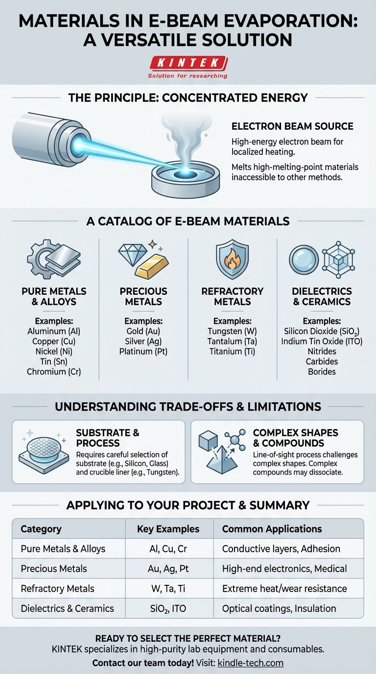
At its core, e-beam evaporation is a highly versatile deposition technique capable of handling a vast array of materials. It is particularly valued for its ability to vaporize materials with high melting temperatures, including pure metals like titanium, refractory metals like tungsten, precious metals like gold and platinum, and dielectric compounds such as silicon dioxide and indium tin oxide.
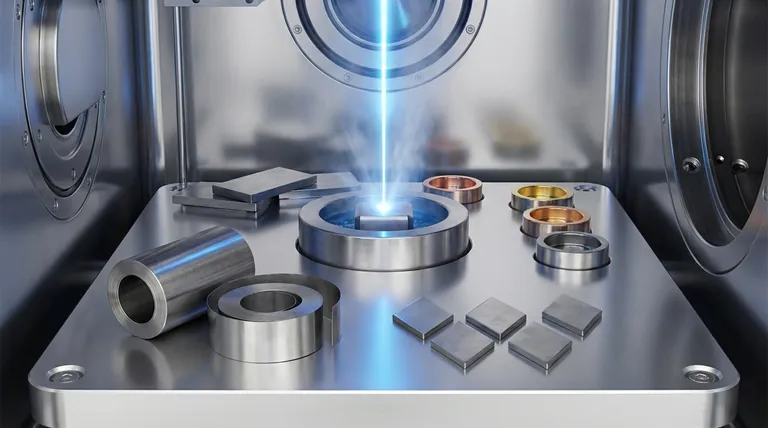
The defining strength of electron-beam evaporation is its use of a focused, high-energy electron beam to vaporize materials. This unlocks the ability to deposit high-melting-point metals and ceramics that are inaccessible to simpler thermal evaporation methods, making it essential for advanced electronics, optics, and high-performance coatings.
The Principle: Why High-Melting-Point Materials Are Key
The unique capability of e-beam evaporation stems directly from how it generates vapor. Understanding this principle explains its material compatibility.
Concentrated Energy for Vaporization
Unlike other methods that heat an entire crucible, an electron beam delivers an immense amount of energy to a very small spot on the source material. This localized heating is efficient enough to melt and vaporize even the most resilient materials.
Overcoming Thermal Barriers
Traditional thermal evaporation struggles with materials like tungsten or tantalum, which have melting points exceeding 3000°C. The e-beam process bypasses this limitation, making it the preferred method for depositing these high-performance films.
A Catalog of E-Beam Evaporation Materials
The range of materials is extensive and can be grouped into several key categories based on their properties and applications.
Pure Metals and Common Alloys
This is the most common category, used for creating conductive layers, reflective surfaces, or adhesion layers.
- Examples: Aluminum (Al), Copper (Cu), Nickel (Ni), Tin (Sn), Chromium (Cr)
Precious Metals
Valued for their conductivity, resistance to oxidation, and biocompatibility, these are critical in high-end electronics and medical devices.
- Examples: Gold (Au), Silver (Ag), Platinum (Pt)
Refractory Metals
These metals are defined by their extreme resistance to heat and wear, making them ideal for demanding aerospace, automotive, and industrial applications.
- Examples: Tungsten (W), Tantalum (Ta), Titanium (Ti)
Dielectrics and Ceramics
These materials are electrical insulators and are often used for their optical properties (like anti-reflection coatings) or as protective, insulating layers in semiconductors.
- Examples: Silicon Dioxide (SiO₂), Indium Tin Oxide (ITO), Nitrides, Carbides, Borides
Understanding the Trade-offs and Limitations
While powerful, e-beam evaporation is not the universal solution for all thin-film needs. Objectivity requires acknowledging its specific constraints.
Substrate and Process Materials
The process involves more than just the material being deposited. The substrate (what is being coated) and the crucible (what holds the source material) are equally important.
- Substrates: Materials like silicon wafers, quartz, sapphire, and glass are common foundations for the thin film.
- Crucibles: The crucible liner must have a higher melting point than the source material. Tungsten and molybdenum are often used for this purpose.
Not Ideal for Certain Compounds
Complex compounds can sometimes break down or "disassociate" under the intense energy of the electron beam. This can alter the composition of the resulting thin film, requiring careful process control.
Line-of-Sight Deposition
E-beam evaporation is a line-of-sight process, meaning the vapor travels in a straight line from the source to the substrate. This makes it challenging to uniformly coat complex, three-dimensional shapes without sophisticated fixtures to rotate the part.
How to Apply This to Your Project
The choice of material is driven entirely by the desired outcome. Your application's requirements will dictate the ideal material to use with the e-beam process.
- If your primary focus is high-performance optics: You will likely use dielectric materials like Silicon Dioxide (SiO₂) or refractory metals like Titanium (Ti) to create precise anti-reflective or reflective coatings.
- If your primary focus is robust electronic conductivity: Precious metals like Gold (Au) or standard metals like Copper (Cu) and Aluminum (Al) are the materials of choice, selected based on cost and performance needs.
- If your primary focus is extreme wear or heat resistance: You should specify refractory metals like Tungsten (W) or ceramics like nitrides and carbides for their inherent durability.
Ultimately, leveraging e-beam evaporation effectively means matching the unique capabilities of the process with the specific material properties your project demands.
Summary Table:
| Material Category | Key Examples | Common Applications |
|---|---|---|
| Pure Metals & Alloys | Aluminum (Al), Copper (Cu), Chromium (Cr) | Conductive layers, adhesion layers |
| Precious Metals | Gold (Au), Silver (Ag), Platinum (Pt) | High-end electronics, medical devices |
| Refractory Metals | Tungsten (W), Tantalum (Ta), Titanium (Ti) | Extreme heat/wear resistance coatings |
| Dielectrics & Ceramics | Silicon Dioxide (SiO₂), Indium Tin Oxide (ITO) | Optical coatings, insulating layers |
Ready to select the perfect material for your e-beam evaporation project?
KINTEK specializes in providing high-purity lab equipment and consumables for precise thin-film deposition. Our experts can help you choose the right materials—from refractory metals to dielectric ceramics—to achieve superior coating performance for your electronics, optics, or industrial applications.
Contact our team today to discuss your specific requirements and discover how KINTEK can support your laboratory's success.
Visual Guide
Related Products
- Electron Beam Evaporation Coating Tungsten Crucible and Molybdenum Crucible for High Temperature Applications
- Electron Beam Evaporation Coating Gold Plating Tungsten Molybdenum Crucible for Evaporation
- Electron Beam Evaporation Coating Oxygen-Free Copper Crucible and Evaporation Boat
- High Purity Pure Graphite Crucible for Electron Beam Evaporation
- Electron Beam Evaporation Coating Conductive Boron Nitride Crucible BN Crucible
People Also Ask
- What is the process of e-beam coating? Achieve High-Purity, Precise Thin Films for Your Lab
- What is the container that holds the metal source material called in e-beam evaporation? Ensure Purity and Quality in Your Thin-Film Deposition
- What is e-beam evaporation? Achieve High-Purity Thin Film Deposition for Your Lab
- What is the deposition rate of e-beam evaporation? Control Thin Film Quality and Speed
- What is e-beam evaporation used for? Precision Coating for Optics, Aerospace & Electronics


