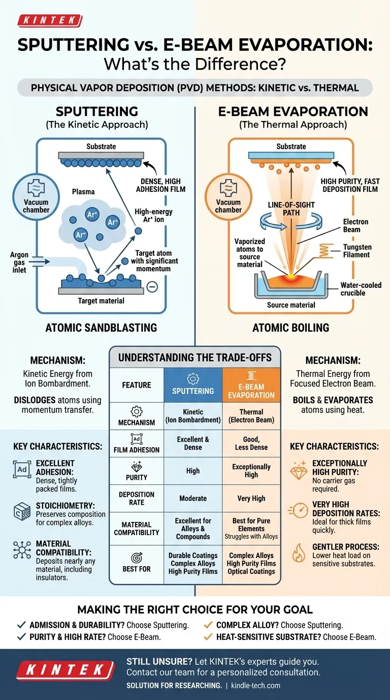
At its core, sputtering and e-beam evaporation are both physical vapor deposition (PVD) methods used to create thin films in a vacuum. The fundamental difference lies in how they liberate atoms from a source material. Sputtering uses kinetic energy from ion bombardment to physically knock atoms off a target, whereas e-beam evaporation uses thermal energy from a focused electron beam to boil and evaporate atoms from a source.
The choice between sputtering and e-beam is a decision between a kinetic process and a thermal one. Sputtering ("atomic sandblasting") excels at creating dense, adhesive films, while e-beam evaporation ("atomic boiling") is superior for high-purity films at very high deposition rates.

How Sputtering Works: The "Kinetic" Approach
Sputtering is best understood as a momentum transfer process. It relies on bombarding a source material, known as the target, with high-energy ions inside a vacuum chamber.
The Sputtering Mechanism
A plasma, typically from an inert gas like Argon, is generated in the chamber. The positively charged Argon ions are accelerated by an electric field and slam into the negatively charged target. This collision has enough energy to physically dislodge or "sputter" atoms from the target's surface. These ejected atoms then travel through the vacuum and deposit onto your substrate, forming a thin film.
Key Characteristics of Sputtered Films
Because the sputtered atoms arrive at the substrate with significant kinetic energy, they form very dense and tightly packed films. This high energy results in excellent adhesion to the substrate. Sputtering is also highly effective for depositing complex materials like alloys or compounds, as it tends to preserve the original material's composition (stoichiometry).
How E-Beam Evaporation Works: The "Thermal" Approach
Electron beam (e-beam) evaporation is a form of thermal evaporation, but one that provides immense energy with surgical precision. It uses a highly focused beam of electrons to heat the source material.
The E-Beam Mechanism
Inside a high-vacuum chamber, a tungsten filament emits a stream of electrons. These electrons are accelerated and guided by magnetic fields to strike a small spot on the source material, which is held in a water-cooled crucible. The intense energy transfer rapidly heats the material past its melting and boiling points, causing it to evaporate. These vaporized atoms travel in a line-of-sight path and condense onto the cooler substrate, forming the film.
Key Characteristics of E-Beam Films
Since the process does not require a carrier gas like Argon, e-beam deposition results in films of exceptionally high purity. It can also achieve very high deposition rates, often an order of magnitude faster than sputtering. The process is "gentler" in some ways, imparting less energy to the growing film, which can be beneficial for sensitive substrates.
Understanding the Trade-offs: Sputtering vs. E-Beam
The differences in their physical mechanisms create a clear set of trade-offs that dictate which process is suitable for a given application.
Film Adhesion and Density
Sputtering almost always produces films with superior adhesion and higher density. The energetic arrival of sputtered atoms helps them embed slightly into the substrate surface and pack together tightly. E-beam films, formed by lower-energy condensation, are generally less dense and have weaker adhesion.
Material Compatibility
Sputtering is highly versatile and can deposit nearly any material, including refractory metals and insulators (with RF sputtering). E-beam is excellent for materials with high melting points but struggles with depositing alloys where the constituent elements have different vapor pressures, as the more volatile element will evaporate first.
Deposition Rate and Control
For many materials, e-beam evaporation offers significantly higher deposition rates than sputtering, making it ideal for creating thick films quickly. Both methods offer precise control over film thickness.
Process Complexity and Cost
As noted in some contexts, sputtering equipment can be relatively simple and robust, especially for basic DC magnetron systems. E-beam systems are generally more complex, requiring high-voltage power supplies, magnetic focusing coils, and more stringent high-vacuum conditions, which can lead to higher maintenance requirements and costs.
Making the Right Choice for Your Goal
Selecting the right technique requires aligning its strengths with your most critical film properties.
- If your primary focus is film adhesion and durability: Choose sputtering for its dense, well-adhered films, ideal for hard coatings or underlayers.
- If your primary focus is material purity and high deposition rates: Choose e-beam evaporation for applications like optical coatings or electronics where purity is paramount.
- If your primary focus is depositing a complex alloy with a specific composition: Sputtering is the more reliable choice to maintain the correct stoichiometry.
- If your primary focus is coating a heat-sensitive substrate: E-beam can sometimes offer a lower overall heat load on the substrate compared to the plasma environment of sputtering.
Ultimately, your material, substrate, and desired film properties will provide the definitive answer.
Summary Table:
| Feature | Sputtering | E-Beam Evaporation |
|---|---|---|
| Mechanism | Kinetic energy (ion bombardment) | Thermal energy (electron beam) |
| Film Adhesion | Excellent, dense films | Good, but generally less dense |
| Purity | High | Exceptionally high (no carrier gas) |
| Deposition Rate | Moderate | Very high |
| Material Compatibility | Excellent for alloys, compounds, and insulators | Best for pure elements; struggles with alloys |
| Best For | Durable coatings, complex alloys, superior adhesion | High-purity films, optical coatings, high deposition rates |
Still unsure which PVD method is right for your application? Let KINTEK's experts guide you to the optimal solution. We specialize in lab equipment and consumables for thin film deposition, helping you achieve the precise film properties your research or production requires.
Contact our team today for a personalized consultation and discover how our sputtering and e-beam evaporation systems can enhance your laboratory's capabilities.
Visual Guide