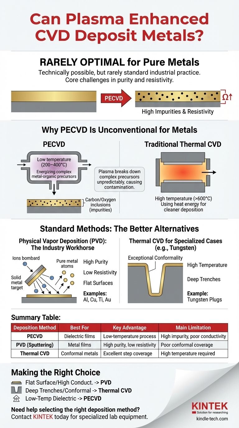
While technically possible in research settings, Plasma Enhanced Chemical Vapor Deposition (PECVD) is rarely the optimal or standard industrial method for depositing pure metal films. The core challenge lies not in the ability to deposit the material, but in achieving the high purity and low electrical resistivity required for most applications. For metallization, other techniques like Physical Vapor Deposition (PVD) or standard thermal CVD are overwhelmingly preferred.
The decision to use PECVD is driven by its low-temperature advantage, which is critical for depositing dielectric films. However, for depositing conductive metals, this advantage is almost always outweighed by the superior film quality, purity, and lower cost offered by methods like sputtering (PVD) or thermal CVD.
Why PECVD Is an Unconventional Choice for Metals
To understand why PECVD isn't a go-to for metals, we must first distinguish it from other deposition methods. The choice of technique is always a function of the material being deposited and the desired properties of the final film.
The Role of Plasma vs. Heat
PECVD uses an energized plasma to break down precursor gases, enabling deposition at low temperatures (typically 200-400°C). This is its defining advantage.
In contrast, traditional thermal CVD uses high temperatures (often >600°C) to supply the energy for the chemical reaction. While hotter, this thermal process can be "cleaner" for certain chemistries.
The Precursor Problem
For CVD of any kind, a volatile precursor gas containing the atom you wish to deposit is required. For metals, these are often complex metal-organic compounds.
In a plasma environment, these complex molecules can shatter in unpredictable ways, leading to the incorporation of carbon or oxygen impurities into the growing film. These impurities dramatically increase the film's electrical resistivity, defeating the purpose of depositing a conductor.
Impact on Film Quality
The primary metric for a metal layer is low resistivity (high conductivity). Due to contamination from precursors, PECVD-deposited metals often have significantly higher resistivity than those deposited by other methods.
Furthermore, the plasma bombardment can sometimes lead to poorer crystal structure and film density, further degrading electrical performance.
Standard Methods for Metal Deposition: The Better Alternatives
Given the limitations of PECVD for metallization, the industry relies on two other primary methods, each with a distinct purpose.
Physical Vapor Deposition (PVD): The Industry Workhorse
PVD, most commonly sputtering, is the default choice for depositing thin metal films like aluminum, copper, titanium, and gold.
In sputtering, ions from a plasma bombard a solid metal target, ejecting atoms that then coat the substrate. This process is clean, fast, and produces very high-purity films with excellent conductivity.
Thermal CVD for Specialized Cases (e.g., Tungsten)
Your reference to Tungsten (W) deposition is a perfect example of where thermal CVD excels. It is used to form conductive plugs that connect different layers of a semiconductor device.
The great advantage of thermal W-CVD is its exceptional conformality—the ability to perfectly coat the bottom and sidewalls of very deep, narrow trenches (high-aspect-ratio features). Line-of-sight PVD methods cannot do this effectively. The high temperatures required for thermal W-CVD are acceptable in these early manufacturing stages.
Understanding the Trade-offs
No deposition technique is universally superior; each involves critical trade-offs. Choosing the right one requires matching the technique's strengths to your application's primary need.
PECVD: Best for Low-Temperature Dielectrics
The key strength of PECVD is its low-temperature process. This makes it the industry standard for depositing dielectric films (e.g., silicon nitride, silicon dioxide) on top of completed device layers that contain metals and cannot withstand high temperatures.
PVD (Sputtering): Best for High-Quality Conductors
PVD is the champion for depositing high-quality, low-resistivity metal films for interconnects and electrodes. Its main limitation is poor coverage over complex, non-planar topography.
Thermal CVD: Best for Conformal Metals
Thermal CVD is a specialized tool used when conformal coverage is the most critical requirement, as in the case of filling deep vias with tungsten. Its high-temperature requirement is its primary drawback.
Making the Right Choice for Your Application
Your choice of deposition method must be guided by the primary requirement of the film you are creating.
- If your primary focus is creating high-conductivity interconnects or electrodes on a mostly flat surface: PVD (sputtering) is the superior and most cost-effective method.
- If you need to fill deep, high-aspect-ratio trenches with a conformal conductive material: Thermal CVD, particularly for tungsten, is the established industry solution.
- If your primary constraint is an extremely low-temperature budget for depositing a dielectric insulator: PECVD is the ideal tool for the job, but it is not a standard choice for pure metals.
Understanding these fundamental trade-offs between deposition mechanisms is the key to selecting the right tool for manufacturing reliable and high-performance devices.
Summary Table:
| Deposition Method | Best For | Key Advantage | Main Limitation |
|---|---|---|---|
| PECVD | Dielectric films | Low-temperature process | High impurity, poor conductivity |
| PVD (Sputtering) | Metal films | High purity, low resistivity | Poor conformal coverage |
| Thermal CVD | Conformal metals | Excellent step coverage | High temperature required |
Need help selecting the right deposition method for your application?
At KINTEK, we specialize in laboratory equipment and consumables for all your thin-film deposition needs. Whether you're working with PVD systems for high-purity metal films or require specialized thermal CVD solutions for conformal coatings, our experts can help you choose the optimal equipment for your specific requirements.
Contact us today to discuss how our solutions can enhance your research and manufacturing processes with reliable, high-performance deposition technology.
Visual Guide
Related Products
- RF PECVD System Radio Frequency Plasma-Enhanced Chemical Vapor Deposition RF PECVD
- Chemical Vapor Deposition CVD Equipment System Chamber Slide PECVD Tube Furnace with Liquid Gasifier PECVD Machine
- Inclined Rotary Plasma Enhanced Chemical Vapor Deposition PECVD Equipment Tube Furnace Machine
- Inclined Rotary Plasma Enhanced Chemical Vapor Deposition PECVD Equipment Tube Furnace Machine
- Microwave Plasma Chemical Vapor Deposition MPCVD Machine System Reactor for Lab and Diamond Growth
People Also Ask
- What is the role of RF-PECVD in VFG preparation? Mastering Vertical Growth and Surface Functionality
- What is plasma enhanced chemical vapour deposition process? Unlock Low-Temperature, High-Quality Thin Films
- What is plasma CVD? Unlock Low-Temperature Thin Film Deposition for Sensitive Materials
- What is plasma chemical vapor deposition? A Low-Temperature Thin Film Coating Solution
- What is plasma enhanced chemical vapour deposition PECVD used for? Enable Low-Temp Thin Films for Electronics & Solar


