At its core, a carbon nanotube's conductivity is determined by its geometry. This property is not inherent to all nanotubes; instead, it arises directly from the specific angle at which the foundational graphene sheet is conceptually "rolled" to form the tube. Depending on this atomic arrangement, known as chirality, a carbon nanotube can behave either as a highly conductive metal or as a semiconductor.
The conductivity of a carbon nanotube is not a fixed property. It is fundamentally dictated by the tube's atomic structure—its chirality—which determines whether its electronic band structure allows it to act like a metal wire or a semiconductor.
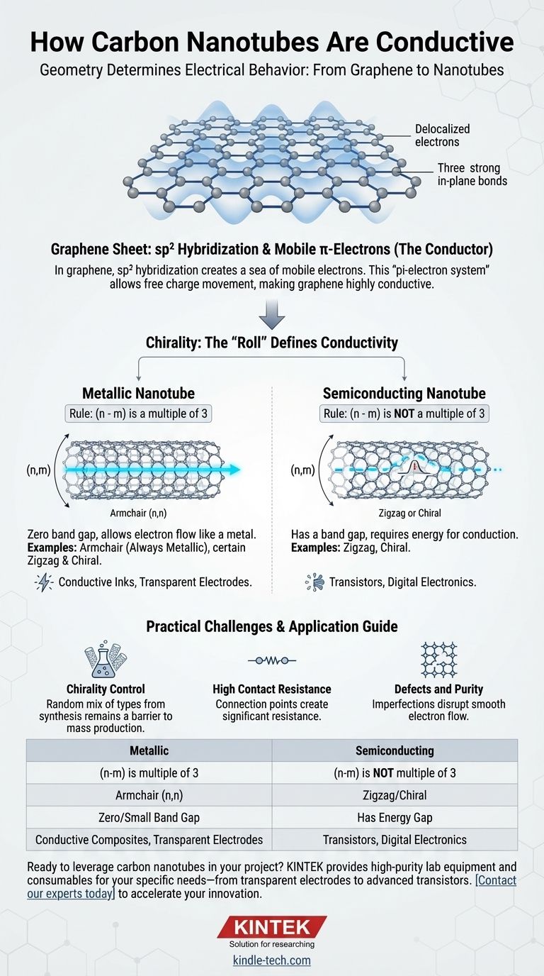
From Graphene to Nanotubes: The Source of Conductivity
To understand why a nanotube conducts electricity, we must first look at its building block: a single, one-atom-thick sheet of carbon called graphene.
The Role of sp² Hybridization
In a graphene sheet, each carbon atom is bonded to three other carbon atoms. This arrangement, known as sp² hybridization, uses three of the carbon's four outer electrons for strong in-plane bonds.
The fourth electron remains in a p-orbital, perpendicular to the graphene sheet. These p-orbitals overlap with their neighbors, creating a delocalized cloud of electrons across the entire sheet.
A "Sea" of Mobile Electrons
This delocalized cloud, or pi-electron system, is not tied to any single atom. These electrons are free to move across the carbon lattice with very little resistance when a voltage is applied.
This is why graphene itself is an exceptionally good electrical conductor. A carbon nanotube is simply a rolled-up version of this highly conductive sheet.
The Critical Factor: Chirality Defines Electrical Behavior
While the potential for conductivity comes from graphene, the actual electrical properties of a specific nanotube are locked in by how that sheet is rolled. This geometric property is called chirality.
What is Chirality?
Chirality is described by a pair of integers (n,m) that define the vector used to roll the graphene sheet into a seamless cylinder. Think of it as the precise angle and circumference of the tube.
This subtle change in the wrapping angle has a profound impact on how the electron waves can travel around the tube's circumference.
Metallic vs. Semiconducting Tubes
The geometry of the roll imposes boundary conditions on the electrons. In some configurations, the electron energy states allow for conduction at any energy level, just like a metal. In others, an energy gap (a band gap) opens up, requiring a small energy input to get electrons moving, which is the definition of a semiconductor.
A simple rule of thumb determines the outcome:
- If (n - m) is a multiple of 3, the nanotube is metallic (or has a very tiny band gap).
- If (n - m) is not a multiple of 3, the nanotube is semiconducting.
Armchair, Zigzag, and Chiral Types
Based on their (n,m) indices, nanotubes are grouped into three main types:
- Armchair (n,n): These tubes are always metallic.
- Zigzag (n,0): These can be metallic or semiconducting depending on the value of n.
- Chiral (n,m): These can be metallic or semiconducting based on the (n-m) rule.
Understanding the Practical Challenges
If some nanotubes are perfect conductors, their practical application is limited by several significant real-world challenges.
The Chirality Control Problem
Current synthesis methods, like Chemical Vapor Deposition (CVD), typically produce a random mix of nanotube types. This "soup" contains a mixture of metallic and semiconducting tubes with different diameters.
For most electronic applications, such as building a transistor, you need purely semiconducting tubes. Separating this mixture is a complex and expensive process that remains a major barrier to mass production.
High Contact Resistance
Even with a perfectly metallic nanotube, getting electricity into and out of the tube is difficult. The connection point between a tiny nanotube and a much larger metal contact creates a significant electrical resistance.
This contact resistance can dominate the overall performance, negating the benefits of the nanotube's excellent intrinsic conductivity.
Defects and Purity
Any defect in the carbon lattice—such as a missing atom or a misplaced bond—can act as a scattering site for electrons. These imperfections disrupt the smooth flow of charge, effectively increasing the tube's resistance.
How to Apply This to Your Project
Your choice of nanotubes depends entirely on your end goal, as different applications have very different requirements for conductivity.
- If your primary focus is high-performance electronics (transistors): You must source pure, single-chirality semiconducting nanotubes to create reliable on/off switching.
- If your primary focus is bulk conductivity (conductive inks, antistatic composites): A mixed-chirality sample is often perfectly acceptable and far more cost-effective, as the metallic tubes form a conductive network.
- If your primary focus is transparent electrodes (solar cells, displays): You need a carefully balanced film that optimizes the trade-off between electrical conductivity (from metallic CNTs) and optical transparency.
Understanding that a nanotube's structure dictates its function is the key to harnessing its remarkable electronic properties.
Summary Table:
| Property | Metallic Nanotube | Semiconducting Nanotube |
|---|---|---|
| Chirality Rule | (n - m) is a multiple of 3 | (n - m) is not a multiple of 3 |
| Example Type | Armchair (n,n) | Zigzag or Chiral (n,m) |
| Band Gap | Zero or very small | Has an energy gap |
| Primary Use | Conductive composites, transparent electrodes | Transistors, digital electronics |
Ready to leverage carbon nanotubes in your project? Whether you need metallic nanotubes for conductive applications or semiconducting tubes for electronics, KINTEK provides high-purity lab equipment and consumables to support your R&D. Our expertise ensures you get the right materials for your specific needs—from transparent electrodes to advanced transistors. Contact our experts today to discuss how we can accelerate your innovation with precision laboratory solutions.
Visual Guide
Related Products
- Carbon Graphite Boat -Laboratory Tube Furnace with Cover
- Boron Nitride (BN) Ceramic Tube
- Hexagonal Boron Nitride HBN Thermocouple Protection Tube
People Also Ask
- What is the disadvantage of graphite furnace? Managing Reactivity and Contamination Risks
- Why is a graphite crucible containing molten bismuth used in LiF–NaF–KF purification? Enhance Melt Purity Efficiently
- Why is graphite used in furnaces? For Extreme Heat, Purity, and Efficiency
- What is the use of graphite tube? Essential for Extreme Heat & Corrosive Environments
- What metals can you melt in a graphite crucible? A Guide to Safe & Efficient Melting