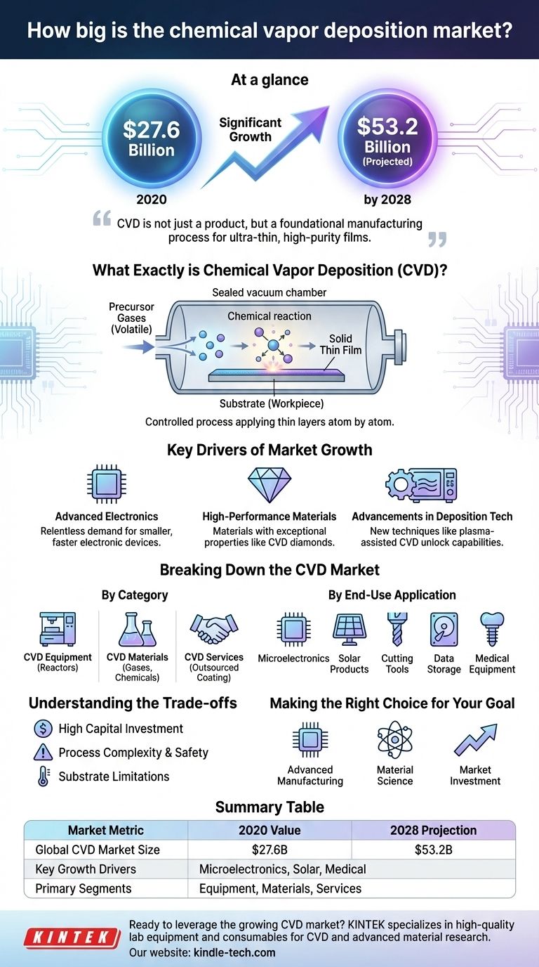
At a glance, the global chemical vapor deposition market was valued at $27.6 billion in 2020 and is projected to nearly double, reaching an estimated $53.2 billion by 2028. This significant growth is a direct reflection of CVD's indispensable role in manufacturing the high-performance components that power modern technology.
The core reason for the market's size and rapid growth is that chemical vapor deposition is not just a single product, but a foundational manufacturing process. It is essential for creating the ultra-thin, highly pure films and coatings required by industries ranging from microelectronics to medical equipment.
What Exactly is Chemical Vapor Deposition?
Chemical vapor deposition, or CVD, is a highly controlled process used to apply a very thin layer of solid material onto a surface, known as a substrate. It is a cornerstone technique for building materials atom by atom.
The Core Process
The entire process takes place within a sealed, vacuumed chamber. This controlled environment is critical for achieving the necessary purity and film quality.
A workpiece or substrate is placed inside the chamber and exposed to specific volatile precursor gases.
A chemical reaction is triggered on the substrate's surface, causing the gases to decompose and deposit a solid, thin film. This reaction "hardens" the material onto the surface, creating the desired coating.
Key Drivers of Market Growth
The expansion of the CVD market isn't driven by a single factor, but by a convergence of demand from several high-tech sectors. Each relies on the unique capabilities that CVD provides.
The Rise of Advanced Electronics
The most significant driver is the relentless demand for smaller, faster, and more powerful electronic devices. CVD is fundamental to manufacturing microelectronics and optoelectronic components.
This process is used to create the intricate layers of silicon, insulators, and conductive metals that form the basis of modern computer chips and data storage devices.
Demand for High-Performance Materials
CVD is used to create materials with exceptional properties, such as extreme hardness, durability, and thermal resistance.
A prime example is the production of CVD diamonds. These lab-grown diamonds are more cost-effective than natural ones and are used in high-endurance cutting tools and advanced optics.
Advancements in Deposition Technology
Continuous innovation in the CVD process itself is unlocking new capabilities.
Techniques like microwave plasma-assisted and thermal-assisted CVD allow for greater control over the properties of the deposited films, opening doors to new applications and improving efficiency.
Breaking Down the CVD Market
To fully understand the market's value, it's helpful to see how it's segmented. The value comes from the equipment used, the materials consumed, and the services provided.
By Category
The market is broadly divided into three main operational segments.
- CVD Equipment: The machinery and reactors required to perform the deposition.
- CVD Materials: The precursor gases and chemicals consumed during the process.
- CVD Services: Companies that provide CVD coating as an outsourced service.
By End-Use Application
The value of CVD is ultimately realized in the final products it helps create.
Key end-use segments include Microelectronics, Solar Products (for anti-reflective coatings), Cutting Tools, Data Storage, and Medical Equipment (for biocompatible coatings).
Understanding the Trade-offs
While powerful, CVD is a sophisticated process with inherent complexities that are important to recognize. It is not a universally applicable solution for all coating needs.
High Capital Investment
CVD reactors and the necessary support systems (like vacuum pumps and gas handling) represent a significant upfront capital expense. This can be a barrier to entry for smaller operations.
Process Complexity and Safety
The process requires precise control over temperature, pressure, and gas flow rates. Furthermore, many precursor gases used in CVD are toxic, flammable, or corrosive, requiring stringent safety protocols.
Substrate Limitations
Traditional CVD often requires very high temperatures, which can damage or deform certain substrate materials. While lower-temperature variants exist (like plasma-enhanced CVD), this remains a key technical consideration.
Making the Right Choice for Your Goal
Understanding the CVD market landscape allows you to identify where the primary opportunities align with your strategic focus.
- If your primary focus is advanced manufacturing: Leveraging CVD services or investing in in-house equipment is critical for producing competitive microelectronics, medical devices, or solar cells.
- If your primary focus is material science: The innovation is in developing new CVD precursor materials that enable novel film properties or create more efficient, safer deposition processes.
- If your primary focus is market investment: The growth in CVD equipment and materials provides a direct opportunity tied to the expansion of the entire semiconductor and high-tech manufacturing ecosystem.
Ultimately, chemical vapor deposition is a critical enabling technology that will continue to grow in importance as our world demands ever more advanced materials.
Summary Table:
| Market Metric | 2020 Value | 2028 Projection |
|---|---|---|
| Global CVD Market Size | $27.6 Billion | $53.2 Billion |
| Key Growth Drivers | Microelectronics, Solar Products, Medical Equipment | |
| Primary Segments | Equipment, Materials, Services |
Ready to leverage the growing CVD market for your lab? KINTEK specializes in providing high-quality lab equipment and consumables essential for CVD processes and advanced material research. Whether you need reactors, precursor materials, or technical support, our solutions are designed to enhance your R&D and manufacturing capabilities. Contact us today to discuss how we can support your laboratory's specific needs and help you stay at the forefront of material science innovation.
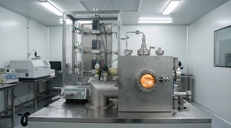
Visual Guide
Related Products
- Chemical Vapor Deposition CVD Equipment System Chamber Slide PECVD Tube Furnace with Liquid Gasifier PECVD Machine
- RF PECVD System Radio Frequency Plasma-Enhanced Chemical Vapor Deposition RF PECVD
- 915MHz MPCVD Diamond Machine Microwave Plasma Chemical Vapor Deposition System Reactor
- Customer Made Versatile CVD Tube Furnace Chemical Vapor Deposition Chamber System Equipment
- Microwave Plasma Chemical Vapor Deposition MPCVD Machine System Reactor for Lab and Diamond Growth
People Also Ask
- How expensive is chemical vapor deposition? Understanding the True Cost of High-Performance Coating
- What are the core advantages of PE-CVD in OLED encapsulation? Protect Sensitive Layers with Low-Temp Film Deposition
- What types of substrates are used in CVD to facilitate graphene films? Optimize Graphene Growth with the Right Catalyst
- What is plasma enhanced chemical vapor deposition PECVD equipment? A Guide to Low-Temperature Thin Film Deposition
- Why is Chemical Vapor Deposition (CVD) equipment uniquely suited for constructing hierarchical superhydrophobic structures?


