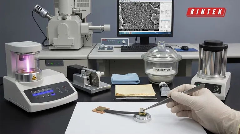
Properly preparing a sample for Scanning Electron Microscopy (SEM) is centered on two fundamental requirements: ensuring the sample is physically sized to fit within the microscope's chamber and making it electrically conductive to prevent image-distorting charge build-up. For materials that are not inherently conductive, this is most often accomplished by applying a thin, conductive coating to the surface.
The core objective of SEM sample preparation is to create a physically stable, electrically conductive target for the electron beam. This prevents imaging artifacts caused by electrical charging and sample movement, which are the most common sources of poor-quality results.
The Two Pillars of SEM Sample Preparation
Effective preparation isn't about a single, complex procedure but rather about satisfying two basic physical principles. Getting these right is essential for acquiring a clear and accurate image.
Pillar 1: Physical Sizing and Stability
The sample must first and foremost fit inside the SEM's vacuum chamber. While this seems obvious, it's a hard physical constraint that dictates the initial preparation steps.
Most SEM chambers accommodate a maximum horizontal dimension of around 10 cm (100 mm) and a vertical height of no more than 40 mm.
Crucially, the sample must be securely mounted to a specimen stub, typically using an adhesive carbon tab or epoxy. Any movement during analysis, even on a microscopic scale, will result in a blurry, unusable image.
Pillar 2: Electrical Conductivity
The SEM works by scanning a focused electron beam across the sample. For a clear image, these electrons must have a path to an electrical ground.
On conductive materials like metals, this happens naturally. However, on insulating samples (e.g., polymers, ceramics, biological specimens), the electrons accumulate on the surface.
This phenomenon, known as "charging," deflects the incoming electron beam, causing severe image distortion, bright patches, and a loss of detail.
To prevent this, insulating samples are coated with a thin layer of a conductive material. This coating provides a path for the electrons to travel from the point of impact to the grounded specimen stub, neutralizing the charge.
Common Pitfalls and Key Decisions
Simply following the steps is not enough; understanding the potential issues and making the right choices for your specific sample is what separates good analysis from bad.
The Problem of Charging Artifacts
If an insulating sample is not coated properly, you will see distinct and disruptive artifacts in your image.
These often appear as exceptionally bright, smeared areas or as horizontal bands that drift across the screen. This is a clear indicator that your sample's conductivity is insufficient.
Choosing the Right Conductive Coating
The most common method for making a sample conductive is sputter coating. The choice of material is critical and depends on your analytical goal.
A thin layer of gold or a gold-palladium alloy is excellent for general high-resolution imaging because it produces a fine-grained, highly conductive film.
However, if you plan to perform elemental analysis (such as EDS/EDX), carbon coating is the preferred method. Gold's own signal can interfere with and mask the signals from elements within your actual sample.
Making the Right Choice for Your Sample
Your preparation strategy should be directly dictated by your sample material and your analytical goals.
- If your sample is inherently conductive (e.g., a metal alloy): Your primary focus is simply on cutting it to the correct size and mounting it securely to the specimen stub.
- If your sample is non-conductive and your goal is high-resolution imaging: You must apply a thin, conductive coating, with gold or gold-palladium being the standard choice.
- If your sample is non-conductive and your goal is elemental analysis: You must use a carbon coat to prevent signal interference that would obscure your results.
By addressing the core needs of physical stability and electrical conductivity, you ensure your sample preparation enables clear, accurate, and insightful analysis.
Summary Table:
| Preparation Step | Key Consideration | Purpose |
|---|---|---|
| Physical Sizing | Max size ~10cm x 40mm | Ensure sample fits in SEM chamber |
| Secure Mounting | Use adhesive carbon tab or epoxy | Prevent sample movement and blurry images |
| Conductive Coating | Gold for imaging; Carbon for EDS/EDX | Prevent charging artifacts and signal interference |
Ready to optimize your SEM sample preparation?
KINTEK specializes in providing high-quality laboratory equipment and consumables, including sputter coaters and mounting supplies, to ensure your SEM analysis is a success. Our experts can help you select the right tools to achieve clear, accurate, and reliable imaging for your specific materials and analytical goals.
Contact our team today to discuss your SEM preparation needs and discover how KINTEK can support your laboratory's success.
Visual Guide

Related Products
- Laboratory Micro Horizontal Jar Mill for Precision Sample Preparation in Research and Analysis
- Vacuum Cold Mounting Machine for Sample Preparation
- Laboratory Grinding Mill Mortar Grinder for Sample Preparation
- Lab Sterile Slapping Type Homogenizer for Tissue Mashing and Dispersing
People Also Ask
- What sample preparation methods are used in labs? Master the Critical First Step for Reliable Analysis
- Why are polyurethane milling jars and corundum balls used for boron carbide? Ensure Purity in Advanced Ceramic Mixing
- What is use for grinding in the laboratory? Select the Right Mill for Accurate Sample Prep
- What is the purpose of sample preparation? Ensure Accurate & Reliable Analytical Results
- What is the use of a laboratory mill? Achieve Accurate Sample Homogenization for Reliable Results