PVD sputtering is a vacuum deposition process that coats a surface by physically ejecting atoms from a source material using high-energy ion bombardment. Think of it as an atomic-scale sandblasting process where energized gas ions, not sand, are used to chip away individual atoms from a target, which then fly across a vacuum chamber and condense onto your part to form an exceptionally thin, uniform, and durable film.
The essential principle of PVD sputtering is momentum transfer. It is a purely physical process—not a chemical or thermal one—that uses a plasma to create high-energy ions that bombard a target, dislodging atoms that then deposit onto a substrate to create a high-performance coating.
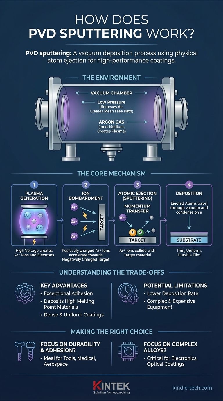
The Environment: Creating the Perfect Conditions
To understand sputtering, you must first understand the environment it requires. The entire process takes place inside a sealed vacuum chamber, which is critical for two reasons.
### The Role of the Vacuum
First, the chamber is pumped down to a very low pressure, removing almost all air and other residual gases. This creates a "mean free path" for atoms to travel from the source to the substrate.
Without a vacuum, the sputtered atoms would simply collide with air molecules and never reach their destination in a controlled manner.
### Introducing the Process Gas
Once a high vacuum is achieved, a small, precisely controlled amount of an inert gas—most commonly Argon—is introduced into the chamber.
This gas is not a reactant; it is the medium that will be used to create the plasma and provide the ions for the bombardment process.
The Core Mechanism: From Plasma to Deposition
With the environment set, the sputtering process itself can begin. It unfolds in a clear, four-step sequence that converts a solid material into a thin film, one atom at a time.
### Step 1: Generating a Plasma
A high voltage is applied within the chamber. This powerful electric field energizes the inert Argon gas, stripping electrons from the Argon atoms.
This creates a plasma, which is a highly ionized state of matter consisting of positively charged Argon ions (Ar+) and free electrons. This plasma often emits a characteristic glow, typically a purple or blue hue.
### Step 2: Ion Bombardment
The source material, known as the target, is given a negative electrical charge. The positively charged Argon ions in the plasma are naturally and aggressively accelerated toward this negatively charged target.
They strike the surface of the target with significant kinetic energy.
### Step 3: Atomic Ejection (Sputtering)
When the high-energy Argon ions collide with the target, they transfer their momentum to the atoms of the target material. This is a purely physical collision, like one billiard ball striking another.
If the momentum transfer is great enough, it knocks atoms loose from the target's surface, ejecting them into the vacuum chamber. This is the "sputtering" effect.
### Step 4: Deposition on the Substrate
The ejected target atoms travel in a straight line through the vacuum until they strike the object being coated, which is called the substrate.
Upon hitting the substrate, they condense and build up, layer by layer, to form a thin, dense, and highly adherent film. Because this happens atom by atom, the process allows for extremely precise control over the coating's thickness and uniformity.
Understanding the Trade-offs
PVD sputtering is a powerful technique, but it's essential to understand its specific advantages and limitations to know when it is the right choice.
### Key Advantages
Sputtering offers exceptional adhesion because the sputtered atoms arrive at the substrate with high energy, embedding themselves slightly into the surface.
The process can be used to deposit materials with very high melting points, such as titanium, chromium, and various ceramics, which are difficult or impossible to deposit using simple thermal evaporation. It also produces coatings that are very dense and uniform.
### Potential Limitations
Compared to other methods like thermal evaporation, sputtering generally has a lower deposition rate, meaning the process can take longer.
The equipment required for sputtering is more complex and expensive due to the need for high-voltage power supplies, vacuum integrity, and process gas control systems.
Making the Right Choice for Your Goal
Selecting a coating process depends entirely on the desired outcome. Sputtering excels in applications where performance and precision are paramount.
- If your primary focus is durability and adhesion: Sputtering is a superior choice for creating hard, dense, and corrosion-resistant films for tools, medical implants, and aerospace components.
- If your primary focus is depositing complex alloys or compounds: Sputtering allows you to maintain the original composition of the source material in the final film, which is critical for advanced electronics and optical coatings.
- If your primary focus is speed and simplicity for a low-melting-point metal: A different PVD method, such as thermal evaporation, might be a more efficient solution.
Ultimately, PVD sputtering provides an unparalleled level of control for engineering high-performance surfaces atom by atom.
Summary Table:
| Process Step | Key Action | Purpose |
|---|---|---|
| 1. Vacuum & Gas | Chamber is evacuated; inert gas (Argon) is introduced. | Creates a clean path for atoms to travel. |
| 2. Plasma Generation | High voltage ionizes the gas, creating a plasma. | Produces the ions needed for bombardment. |
| 3. Ion Bombardment | Positively charged ions accelerate toward the negatively charged target. | Transfers energy to the target material. |
| 4. Atomic Ejection | Ions collide with the target, physically ejecting atoms. | The "sputtering" event that creates the coating material. |
| 5. Film Deposition | Ejected atoms travel and condense on the substrate. | Forms a thin, uniform, and highly adherent coating. |
Need a High-Performance Coating Solution?
PVD sputtering is ideal for creating durable, precise thin films for applications in optics, electronics, medical devices, and tooling. KINTEK specializes in advanced lab equipment, including PVD systems, to help you achieve superior coating results.
Contact our experts today to discuss how our solutions can meet your specific laboratory needs and enhance your research and development capabilities.
Visual Guide
Related Products
- Inclined Rotary Plasma Enhanced Chemical Vapor Deposition PECVD Equipment Tube Furnace Machine
- Vacuum Hot Press Furnace Machine for Lamination and Heating
- 915MHz MPCVD Diamond Machine Microwave Plasma Chemical Vapor Deposition System Reactor
- HFCVD Machine System Equipment for Drawing Die Nano-Diamond Coating
- Laboratory Sterilizer Lab Autoclave Pulse Vacuum Lifting Sterilizer
People Also Ask
- What is the difference between PECVD and CVD? Unlock the Right Thin-Film Deposition Method
- What is the difference between CVD and PECVD? Choose the Right Thin-Film Deposition Method
- What materials are deposited in PECVD? Discover the Versatile Thin-Film Materials for Your Application
- What is PECVD used for? Achieve Low-Temperature, High-Performance Thin Films
- What is plasma enhanced chemical vapour deposition process? Unlock Low-Temperature, High-Quality Thin Films