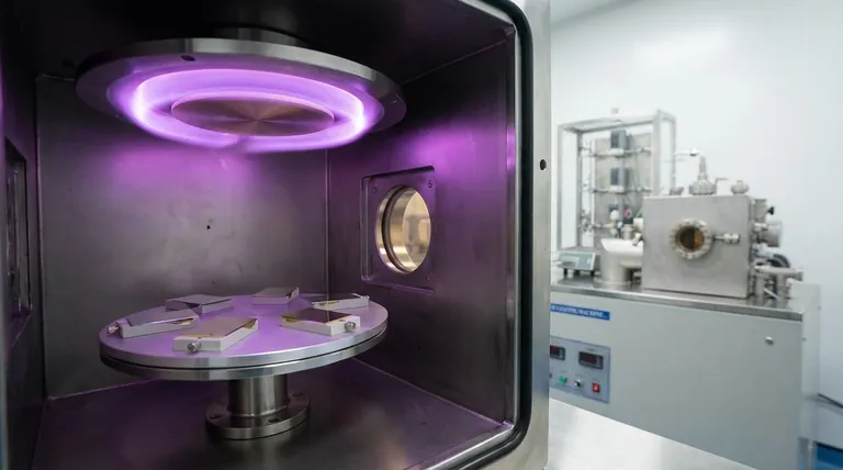
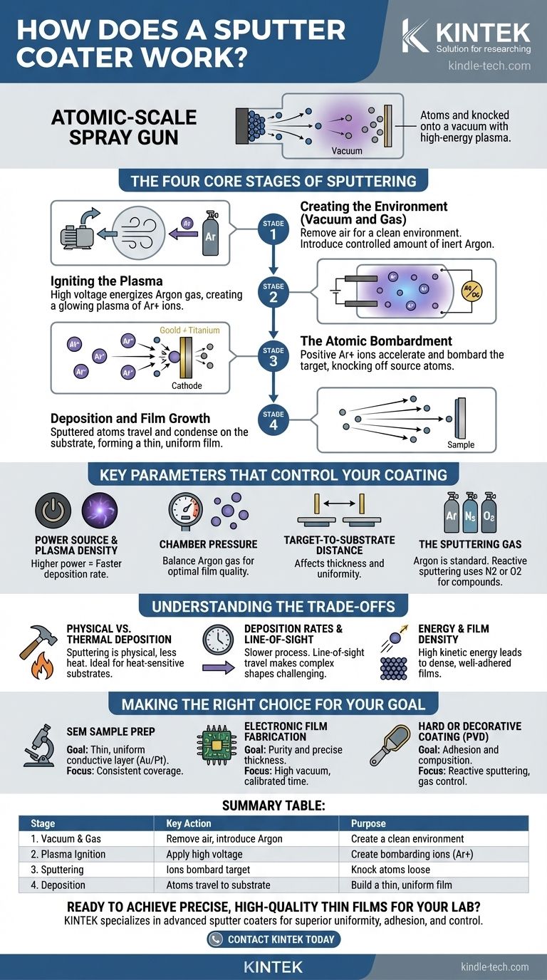
At its core, a sputter coater is an atomic-scale spray gun that physically knocks atoms off a source material and deposits them as an ultra-thin film onto a sample. This process occurs within a vacuum and uses high-energy plasma to bombard the source, creating a controlled, uniform coating.
Sputter coating is not a thermal process of melting or boiling a material. Instead, it is a purely physical phenomenon—a high-energy game of atomic billiards—where ions are used to precisely chip atoms away from a target, which then build up as a thin film on your substrate.
The Four Core Stages of Sputtering
To understand how a sputter coater works, it's best to break it down into four distinct, sequential stages. This entire process happens inside a sealed chamber.
Stage 1: Creating the Environment (Vacuum and Gas)
First, a vacuum pump removes the air from the sample chamber. This is critical because air molecules would interfere with the process, scattering the sputtered atoms and contaminating the final film.
Once a low pressure is achieved, a small, controlled amount of an inert gas, almost always Argon, is introduced into the chamber.
Stage 2: Igniting the Plasma
A high voltage (either DC or RF) is applied between two electrodes in the chamber. The target (the material you want to coat with, like gold or titanium) acts as the negative electrode (cathode).
This strong electric field energizes the Argon gas, stripping electrons from the Argon atoms and creating a plasma—a glowing, ionized gas consisting of positive Argon ions (Ar+) and free electrons.
Stage 3: The Atomic Bombardment
The positively charged Argon ions are powerfully attracted to the negatively charged target. They accelerate towards the target and collide with its surface with tremendous force.
This high-energy impact is strong enough to physically knock atoms loose from the target material. This ejection of target atoms is the "sputtering" effect.
Stage 4: Deposition and Film Growth
The newly sputtered atoms from the target travel through the low-pressure chamber in straight lines.
When these atoms reach your sample (the substrate), they land and condense on its surface. Over seconds or minutes, these atoms build up layer by layer, forming a thin, uniform, and high-purity film.
Key Parameters That Control Your Coating
The quality, thickness, and deposition rate of the sputtered film are not accidental. They are directly controlled by several key parameters of the machine.
The Power Source and Plasma Density
The voltage and current applied to the target determine the energy of the bombarding ions and the density of the plasma. Higher power generally results in a faster deposition rate.
Chamber Pressure
The amount of Argon gas in the chamber is a delicate balance. Too much gas (high pressure) will cause sputtered atoms to collide with gas molecules and scatter before reaching the substrate, leading to a poor-quality film. Too little gas (low pressure) makes it difficult to sustain a stable plasma.
Target-to-Substrate Distance
The distance between the source material and your sample affects both the thickness and the uniformity of the coating. A greater distance can improve uniformity but will also decrease the deposition rate, requiring longer process times.
The Sputtering Gas
While Argon is the standard due to its ideal mass and chemical inertness, other gases can be used for specific purposes. In a process called reactive sputtering, a gas like nitrogen or oxygen is added to form a compound coating (e.g., Titanium Nitride) on the substrate.
Understanding the Trade-offs
Sputtering is a powerful technique, but it's essential to understand its inherent characteristics to use it effectively.
Physical vs. Thermal Deposition
Because sputtering is a physical "knock-off" process, it generates much less radiant heat than thermal evaporation, where the source material is melted. This makes sputtering ideal for coating heat-sensitive substrates like plastics or biological samples.
Deposition Rates and Line-of-Sight
Sputtering is generally a slower process than thermal evaporation. The atoms travel in a line-of-sight path, so coating complex, three-dimensional shapes with deep crevices can be challenging without sample rotation.
Energy and Film Density
The sputtered atoms arrive at the substrate with significant kinetic energy. This helps them form a dense, well-adhered film with excellent structural properties, which is often superior to films from other deposition methods.
Making the Right Choice for Your Goal
The ideal settings for your sputter coater depend entirely on your objective.
- If your primary focus is preparing samples for SEM (Scanning Electron Microscopy): Your goal is a thin, uniform, conductive layer (like gold or platinum) to prevent electron charging, so focus on achieving consistent, complete coverage rather than high speed.
- If your primary focus is fabricating a functional electronic film: Purity and precise thickness are paramount, so ensure a high vacuum, use high-purity gas, and carefully calibrate your deposition time and power.
- If your primary focus is creating a hard or decorative coating (PVD): Film adhesion and specific chemical composition are key, often requiring reactive sputtering and careful control over the mix of inert and reactive gases.
By understanding the process as a controlled atomic bombardment, you can adjust each parameter to precisely engineer the thin film your work requires.
Summary Table:
| Stage | Key Action | Purpose |
|---|---|---|
| 1. Vacuum & Gas | Remove air, introduce Argon | Create a clean, interference-free environment |
| 2. Plasma Ignition | Apply high voltage to target | Ionize gas to create bombarding ions (Ar+) |
| 3. Sputtering | Ions bombard target (cathode) | Knock atoms loose from the source material |
| 4. Deposition | Sputtered atoms travel to substrate | Build a thin, uniform, high-purity film layer by layer |
Ready to achieve precise, high-quality thin films for your lab?
KINTEK specializes in advanced sputter coaters and lab equipment designed for researchers and technicians who demand superior film uniformity, adhesion, and control—whether for SEM sample preparation, electronics fabrication, or specialized PVD coatings.
Our experts can help you select the ideal system for your specific materials and application goals. Contact KINTEK today to discuss your project and see how our solutions can enhance your research and development.
Visual Guide
Related Products
- Custom CVD Diamond Coating for Lab Applications
- HFCVD Machine System Equipment for Drawing Die Nano-Diamond Coating
- Chemical Vapor Deposition CVD Equipment System Chamber Slide PECVD Tube Furnace with Liquid Gasifier PECVD Machine
- Multifunctional Electrolytic Electrochemical Cell Water Bath Single Layer Double Layer
- Professional Cutting Tools for Carbon Paper Cloth Diaphragm Copper Aluminum Foil and More
People Also Ask
- What are the advantages of CVD coating? Superior Hardness and Uniformity for Demanding Applications
- What is CVD coating? Transform Your Material's Surface for Maximum Performance
- Can you coat something in diamond? Unlock Unmatched Hardness and Thermal Conductivity
- What is CVD diamond coating? Grow a Super-Hard, High-Performance Diamond Layer
- What is the use of CVD coating? Enhance Durability and Functionality for Your Components


