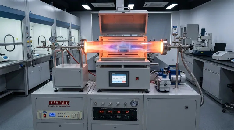
In essence, Chemical Vapor Deposition (CVD) is a process that 'grows' a coating directly onto a material's surface through a controlled chemical reaction. Inside a heated, vacuum-sealed chamber, volatile precursor gases are introduced. These gases react or decompose upon contact with the hot substrate, depositing a thin, solid film that chemically bonds to the surface. The remaining gaseous byproducts are then safely removed.
CVD is not merely applying a layer; it's a high-temperature chemical synthesis that transforms a gas into a solid film directly on a component. This creates an exceptionally well-bonded, uniform coating on even the most complex shapes, but its high heat requirement is the primary constraint on which materials can be treated.
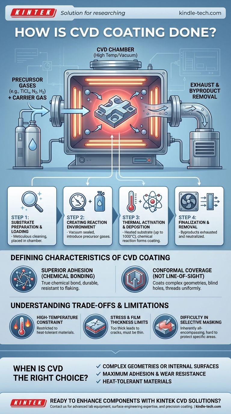
The CVD Process: A Step-by-Step Breakdown
The CVD process is a precise, multi-stage operation conducted within a specialized reactor. Each step is critical to forming a high-quality, high-purity film.
Step 1: Substrate Preparation and Loading
Before any coating can occur, the substrate—the part being coated—must be meticulously cleaned to remove any contaminants.
The prepared substrate is then placed inside the reaction chamber. The integrity of the final coating depends entirely on this initial surface purity.
Step 2: Creating the Reaction Environment
The chamber is sealed and air is pumped out to create a vacuum. This removes unwanted atmospheric gases that could interfere with the reaction.
Once under vacuum, a carefully controlled mixture of one or more volatile precursor gases is introduced. These are the gases that contain the elements needed for the final coating. An inert carrier gas is often used to help transport them.
Step 3: Thermal Activation and Deposition
The substrate is heated to a specific, often very high temperature, sometimes up to 1000°C (1832°F).
This intense heat provides the energy needed to trigger a chemical reaction. The precursor gases either decompose or react with each other at the hot surface of the substrate.
As the gases react, they form a solid material that deposits onto the substrate, atom by atom, building a thin, dense, and uniform film. For example, a mixture of Titanium Tetrachloride (TiCl₄), Nitrogen (N₂), and Hydrogen (H₂) will react to form a hard Titanium Nitride (TiN) coating.
Step 4: Finalization and Byproduct Removal
The chemical reaction also produces volatile byproducts, which remain in a gaseous state.
These byproducts are continuously drawn out of the chamber by the vacuum system. They are then processed to neutralize any hazardous materials before being safely vented.
The Defining Characteristics of a CVD Coating
The method by which a CVD coating is formed gives it distinct and valuable properties that differentiate it from other surface treatments.
Superior Adhesion via Chemical Bonding
Unlike paint or simple plating, a CVD coating is not just sitting on top of the material. The process creates a true chemical bond between the coating and the substrate.
This results in exceptional adhesion, making the coating extremely durable and resistant to flaking or chipping. It effectively becomes an integral part of the component's surface.
Conformal Coverage (Not Line-of-Sight)
Because the coating is formed from a gas that fills the entire chamber, it can penetrate and coat all exposed areas of a part uniformly.
This is a major advantage over "line-of-sight" processes like Physical Vapor Deposition (PVD). CVD can easily coat complex geometries, blind holes, threads, and even internal surfaces with a consistent thickness.
Understanding the Trade-offs and Limitations
While powerful, CVD is not a universal solution. Its process conditions create important trade-offs that must be considered.
The High-Temperature Constraint
The very high temperatures required for the reaction are the single greatest limitation of CVD.
This restricts the process to substrate materials that can withstand the heat without melting, warping, or having their fundamental properties (like temper) negatively altered.
Stress and Film Thickness Limits
As the coating builds up, internal stresses can develop within the film.
If the coating becomes too thick, this stress can exceed the material's strength, leading to cracks or delamination. Therefore, most CVD coatings are, by necessity, very thin films.
Difficulty in Selective Masking
Since the reactive gas will coat any heated surface it can reach, it is very difficult to "mask off" or protect specific areas of a component that should not be coated. The process is inherently all-encompassing.
When is CVD the Right Choice?
Choosing a coating technology requires matching the process capabilities to your primary engineering goal.
- If your primary focus is coating complex geometries or internal surfaces: CVD is often the superior choice due to its non-line-of-sight, conformal nature.
- If your primary focus is maximum adhesion and wear resistance on a heat-tolerant material: The chemical bond formed by CVD provides exceptional performance and durability.
- If you are working with temperature-sensitive materials (like certain aluminum alloys or tempered steels): You must explore alternative, lower-temperature processes, as CVD's high heat can be detrimental.
Ultimately, selecting CVD is a decision to leverage its unparalleled adhesion and conformal coverage, provided your material can withstand the demanding thermal environment of the process.
Summary Table:
| Key Aspect | Description |
|---|---|
| Process Type | High-temperature chemical reaction converting gas to solid film |
| Primary Advantage | Conformal, uniform coverage on complex geometries and internal surfaces |
| Adhesion Quality | True chemical bonding for exceptional durability |
| Temperature Range | Up to 1000°C (1832°F) |
| Best For | Heat-tolerant materials requiring maximum wear resistance |
| Limitation | Not suitable for temperature-sensitive substrates |
Ready to enhance your components with high-performance CVD coatings?
At KINTEK, we specialize in advanced lab equipment and consumables for surface engineering applications. Our expertise in CVD technology can help you achieve:
- Exceptional wear resistance for longer component lifespan
- Uniform coverage on even the most complex geometries
- Superior chemical bonding that prevents flaking and chipping
- Precision coating solutions tailored to your specific material requirements
Whether you're working with cutting tools, aerospace components, or specialized industrial parts, our team can provide the equipment and support you need for successful CVD applications.
Contact KINTEK today to discuss how our CVD solutions can solve your toughest surface engineering challenges and deliver reliable, high-performance results for your laboratory or manufacturing needs.
Visual Guide
Related Products
- Custom CVD Diamond Coating for Lab Applications
- HFCVD Machine System Equipment for Drawing Die Nano-Diamond Coating
- Laboratory CVD Boron Doped Diamond Materials
- CVD Diamond for Thermal Management Applications
- CVD Diamond Dressing Tools for Precision Applications
People Also Ask
- What is the use of CVD coating? Enhance Durability and Functionality for Your Components
- How thick is CVD diamond coating? Balancing Durability and Stress for Optimal Performance
- What is CVD coating? Transform Your Material's Surface for Maximum Performance
- What is CVD coated? A Guide to Superior Wear Resistance for Complex Parts
- What is CVD coating used for? Hardening Tools & Building Semiconductors for Industry


