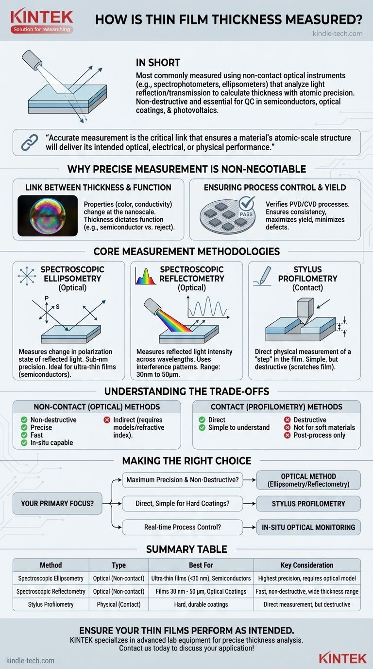
In short, thin film thickness is most commonly measured using non-contact optical instruments, such as spectrophotometers or ellipsometers. These tools analyze how light reflects off or passes through the film, using the properties of the light waves to calculate thickness with incredible precision, often down to the atomic level. This non-destructive method is essential for quality control in industries like semiconductors, optical coatings, and photovoltaics.
The core challenge isn't just finding a tool to measure thickness; it's understanding that a film's thickness is inseparable from its function. Accurate measurement is the critical link that ensures a material's atomic-scale structure will deliver its intended optical, electrical, or physical performance.
Why Precise Measurement is Non-Negotiable
The function of a thin film is often dictated entirely by its thickness. A few nanometers can be the difference between a functional semiconductor and a reject, or an anti-reflection coating and a simple mirror.
The Link Between Thickness and Function
A material's properties change at the nanoscale. The color, transparency, conductivity, and hardness of a thin film are directly governed by its thickness and uniformity.
For example, the vibrant, shifting colors on a soap bubble are caused by light waves reflecting off the inner and outer surfaces of its thin film. The film's varying thickness creates interference patterns that we perceive as color. Optical coatings work on the exact same principle.
Ensuring Process Control and Yield
Thin films are created using highly controlled vacuum deposition processes like Physical Vapor Deposition (PVD) or Chemical Vapor Deposition (CVD).
Measuring thickness verifies that these expensive and sensitive processes are operating correctly. It allows manufacturers to ensure consistency, maximize product yield, and minimize costly defects.
Core Measurement Methodologies
While several methods exist, they generally fall into two categories: optical (non-contact) and physical (contact).
Spectroscopic Ellipsometry
This advanced optical technique measures the change in the polarization of light as it reflects off the thin film.
By analyzing how the light's polarization state shifts, ellipsometry can determine thickness with sub-nanometer precision. It is extremely powerful for measuring ultra-thin films used in semiconductor devices.
Spectroscopic Reflectometry
This method, often performed with a spectrophotometer, measures the amount of light reflected from a film over a range of wavelengths.
The reflected light creates an interference pattern, similar to the colors on an oil slick. By analyzing the peaks and valleys in this pattern, software can accurately calculate the film's thickness. This is widely used for films between 30 nanometers and 50 micrometers.
Stylus Profilometry (Contact Method)
This is a direct, physical measurement. It requires creating a "step" in the film down to the bare substrate.
A very fine diamond-tipped stylus is then dragged across the step. The physical change in the stylus's vertical position directly reveals the film's thickness.
Understanding the Trade-offs
Choosing a measurement method involves balancing the need for precision against practical constraints like cost, speed, and whether the sample can be touched.
Non-Contact (Optical) Methods: Precision vs. Complexity
Pros: These methods are non-destructive, extremely precise, and very fast. They can also be integrated directly into the manufacturing process for real-time monitoring.
Cons: They are indirect measurements that rely on mathematical models. Accurate results require knowing the optical properties (refractive index) of the film material.
Contact (Profilometry) Methods: Simplicity vs. Destruction
Pros: This technique provides a direct, unambiguous measurement that is easy to understand and less dependent on material properties.
Cons: It is a destructive test, as it requires scratching the film to create a step. It cannot be used on soft materials and can only be performed after the product is made, not during the process.
Making the Right Choice for Your Goal
Your application's requirements will dictate the best measurement strategy.
- If your primary focus is maximum precision and non-destructive analysis for optical or semiconductor applications: Your best choice is a non-contact optical method like spectroscopic ellipsometry or reflectometry.
- If your primary focus is a direct, simple measurement for hard, durable coatings where a small test area can be sacrificed: Stylus profilometry is a reliable and straightforward option.
- If your primary focus is real-time control over a deposition process to improve yield and consistency: An in-situ optical monitoring system is the only effective solution.
Ultimately, selecting the right measurement technique is fundamental to translating material science into reliable, high-performance products.
Summary Table:
| Method | Type | Best For | Key Consideration |
|---|---|---|---|
| Spectroscopic Ellipsometry | Optical (Non-contact) | Ultra-thin films (<30 nm), Semiconductors | Highest precision, requires optical model |
| Spectroscopic Reflectometry | Optical (Non-contact) | Films 30 nm - 50 μm, Optical Coatings | Fast, non-destructive, wide thickness range |
| Stylus Profilometry | Physical (Contact) | Hard, durable coatings | Direct measurement, but destructive |
Ensure your thin films perform as intended. The right thickness measurement is critical for the success of your semiconductor, optical coating, or photovoltaic project. At KINTEK, we specialize in providing advanced lab equipment and consumables tailored to your laboratory's precise needs. Let our experts help you select the perfect tool for accurate, reliable thickness analysis. Contact us today to discuss your application and elevate your process control!
Visual Guide