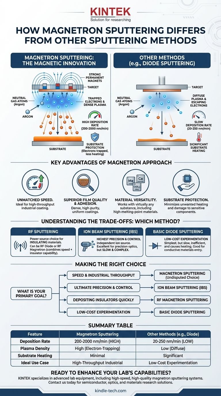
The fundamental difference is the use of a magnetic field. Magnetron sputtering strategically places strong magnets behind the target material, which traps electrons in a dense plasma cloud directly in front of the target. This concentrated plasma bombards the target far more intensely than in other sputtering methods, resulting in significantly higher deposition rates—often an order of magnitude faster.
While all sputtering methods eject atoms from a target to create a thin film, magnetron sputtering's use of a magnetic field is the key innovation. This single change dramatically increases the speed and efficiency of the deposition process, establishing it as the dominant technique for most industrial applications.
The Core Mechanism: How Magnets Revolutionize Sputtering
To understand the difference, we must first look at the core challenge of basic sputtering. The process relies on a plasma—an ionized gas—to create ions that bombard a source material, or "target."
The Problem with Basic Sputtering
In a simple diode sputtering system, the plasma is diffuse and inefficient. Electrons, which are crucial for creating the ions that do the sputtering, are free to escape and often bombard the substrate, potentially causing damage and heating. This results in a slow deposition rate.
The Magnetron Solution: Trapping Electrons
Magnetron sputtering introduces a powerful magnetic field directly behind the target. This field is perpendicular to the electric field, forcing the highly energetic secondary electrons into a spiral path, effectively trapping them near the target's surface.
This confinement prevents electrons from escaping to the substrate and drastically increases their path length within the plasma.
The Result: A High-Density Plasma
Because the electrons are trapped and travel much farther, they cause significantly more ionization events with the neutral gas atoms (like Argon). This creates a much denser, more intense plasma localized directly in front of the target.
This high-density plasma generates a massive flux of ions that continuously bombard the target, ejecting material at a very high rate.
Key Advantages of the Magnetron Approach
The use of a magnetic field delivers several distinct and powerful advantages over more basic sputtering methods.
Unmatched Deposition Speed
The primary benefit is a dramatic increase in the coating rate. As the references show, magnetron sputtering can achieve rates of 200-2000 nm/min, compared to the 20-250 nm/min typical of standard RF sputtering. This makes it ideal for industrial-scale production where throughput is critical.
Superior Film Quality and Adhesion
Sputtered atoms inherently have higher kinetic energy than evaporated materials, which helps create dense films with excellent adhesion. Magnetron sputtering enhances this by maintaining a stable, high-purity process that produces uniform coatings.
Material Versatility
Because sputtering is a physical process and does not require melting the source material, it works with virtually any substance. This includes metals, alloys, ceramics, and materials with extremely high melting points that are impossible to deposit via thermal evaporation.
Substrate Protection
By confining electrons near the target, magnetron sputtering prevents them from striking the substrate. This minimizes unwanted heating and potential radiation damage, which is especially important for sensitive substrates like plastics or electronic components.
Understanding the Trade-offs: Magnetron vs. Other Methods
While magnetron sputtering is a superior technique for many applications, it is not the only option. The choice depends on your specific goals for precision, material, and cost.
Compared to Basic Diode Sputtering
Diode sputtering is the simplest form, without magnetic confinement. It is slow, inefficient, and creates significant substrate heating. Magnetron sputtering is a direct and vast improvement for nearly every metric, especially speed and film quality.
Compared to RF Sputtering
Radio Frequency (RF) sputtering is not a separate method so much as a power source choice. It is required to sputter insulating (dielectric) materials. You can have RF Diode Sputtering or RF Magnetron Sputtering. Combining an RF power supply with a magnetron source gives you the speed of magnetron with the ability to deposit insulators.
Compared to Ion Beam Sputtering (IBS)
Ion Beam Sputtering offers the highest degree of control. In IBS, the ion source is separate from the target, allowing for independent control over ion energy, angle, and flux. This provides unparalleled precision for creating extremely dense, smooth, and stress-controlled films for high-end applications like precision optics.
The trade-off is speed and cost. IBS is significantly slower and more complex than magnetron sputtering, making it less suitable for high-volume production.
Making the Right Choice for Your Application
Selecting the correct sputtering method requires aligning the technique's strengths with your project's primary objective.
- If your primary focus is speed and industrial throughput: Magnetron sputtering is the undisputed choice for its high deposition rates and cost-effectiveness.
- If your primary focus is ultimate film density and precision control: Ion Beam Sputtering (IBS) provides the fine-tuning necessary for sensitive optical coatings and advanced semiconductor films.
- If your primary focus is depositing insulating materials quickly: RF Magnetron Sputtering combines the capability of RF with the speed of a magnetron, offering the best of both worlds.
- If your primary focus is low-cost experimentation on conductive materials: A simple DC diode sputtering setup can be a viable, albeit slow, entry point.
Ultimately, understanding the role of the magnetic field empowers you to select the right tool for the job.
Summary Table:
| Feature | Magnetron Sputtering | Other Methods (e.g., Diode Sputtering) |
|---|---|---|
| Deposition Rate | 200-2000 nm/min | 20-250 nm/min |
| Plasma Density | High (electron-trapping) | Low (diffuse) |
| Substrate Heating | Minimal | Significant |
| Ideal Use Case | High-throughput industrial coatings | Low-cost experimentation |
Ready to enhance your lab's thin-film capabilities? KINTEK specializes in advanced lab equipment, including magnetron sputtering systems designed for high deposition rates and superior film quality. Whether you're in semiconductor manufacturing, optics, or materials research, our solutions deliver precision and efficiency. Contact us today to find the perfect sputtering system for your laboratory needs!
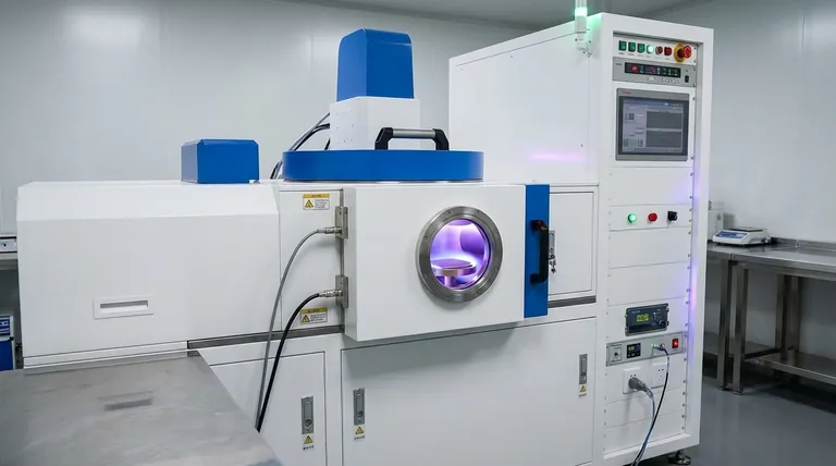
Visual Guide
Related Products
- Microwave Plasma Chemical Vapor Deposition MPCVD Machine System Reactor for Lab and Diamond Growth
- Chemical Vapor Deposition CVD Equipment System Chamber Slide PECVD Tube Furnace with Liquid Gasifier PECVD Machine
- Molybdenum Tungsten Tantalum Special Shape Evaporation Boat
- Inclined Rotary Plasma Enhanced Chemical Vapor Deposition PECVD Equipment Tube Furnace Machine
- Inclined Rotary Plasma Enhanced Chemical Vapor Deposition PECVD Equipment Tube Furnace Machine
People Also Ask
- What is microwave plasma chemical vapor deposition? A Guide to High-Purity Diamond Film Growth
- How is a diamond formed from CVD? The Science of Growing Diamonds Atom by Atom
- What are the advantages of a Microwave Plasma CVD reactor for MCD/NCD coatings? Precision Multilayer Diamond Engineering
- Why is argon-rich gas phase chemistry used for UNCD growth? Unlock Precision Nano-Diamond Synthesis
- How do vacuum pumps and valves collaborate in MPCVD? Achieve Precise Pressure Control for Superior CNT Synthesis