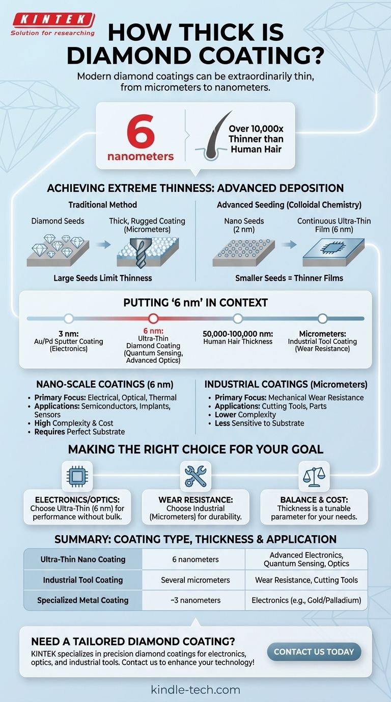
In short, modern diamond coatings can be extraordinarily thin. With recent advancements in deposition technology, it is now possible to produce uniform diamond coatings as thin as 6 nanometers. For scale, this is over 10,000 times thinner than a human hair.
The key takeaway is that "diamond coating" does not refer to a single thickness. The technology has evolved to a point where thickness is a precisely engineered parameter, ranging from several micrometers for industrial tools down to just a few nanometers for advanced electronics.
How Such Extreme Thinness is Achieved
The ability to create such ultra-thin films is not about simply applying a thinner layer. It relies on fundamentally new approaches to how the diamond is grown on a surface.
The Role of Diamond "Seeds"
Diamond coatings are not "painted on." Instead, they are grown in a process called chemical vapor deposition (CVD), which starts with nano-sized diamond particles, or "seeds," distributed on a surface. The final film grows from and connects these initial seeds.
Advanced Seeding Techniques
Historically, achieving a thin, continuous film was limited by the size of the initial diamond seeds. If the seeds are too large, the coating must be thick just to cover them and form a complete layer.
Recent breakthroughs use sophisticated methods, such as colloidal chemistry and the air oxidation of diamond particles, to dramatically reduce the seed size.
From 2 nm Seeds to a 6 nm Film
These advanced methods can produce diamond seed particles as small as 2 nanometers. Starting with such incredibly small and uniform seeds allows for the growth of a complete, continuous diamond film that is only 6 nanometers thick.
Putting "6 Nanometers" in Context
A 6 nm coating is a remarkable achievement that opens up entirely new applications for diamond's unique properties.
Comparison with Other Nanocoatings
This level of thinness places diamond coatings in the same category as other high-performance thin films. For perspective, specialized Gold/Palladium coatings used in electronics can be sputtered onto wafers at a thickness of just 3 nanometers.
Industrial vs. Nano-Scale Coatings
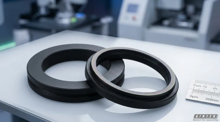
It's important to distinguish these nano-scale films from more traditional diamond coatings. The thick, rugged coatings used on cutting tools or wear-resistant parts are often measured in micrometers (thousands of nanometers), not single-digit nanometers.
The Impact on New Applications
An ultra-thin, perfectly uniform diamond layer enables technologies that were previously impossible. This includes applications in advanced semiconductors, quantum sensing, biocompatible implants, and high-performance optics where adding any significant bulk is not an option.
Understanding the Trade-offs
While incredibly thin coatings are a major advancement, the choice of thickness always involves balancing competing factors.
Thickness vs. Durability
An ultra-thin 6 nm film, while fully continuous, will not provide the same level of abrasion resistance as a 10-micrometer-thick coating on a drill bit. The primary function of nano-scale films is often electrical, thermal, or optical, not heavy-duty mechanical protection.
Complexity and Cost
The advanced colloidal chemistry and deposition methods required to produce nano-scale films are significantly more complex and costly than the processes used for creating thicker, industrial-grade coatings.
Substrate and Uniformity
At the nanometer scale, the smoothness and cleanliness of the underlying material (the substrate) become critically important. Achieving a perfectly uniform 6 nm film requires an equally perfect surface to build upon.
Making the Right Choice for Your Goal
The ideal thickness of a diamond coating is entirely dependent on the problem you are trying to solve.
- If your primary focus is advanced electronics, optics, or sensors: The availability of ultra-thin coatings (in the 6 nm range) is a critical enabling technology.
- If your primary focus is mechanical wear resistance for tools or parts: A much thicker coating, likely measured in micrometers, will be necessary to ensure durability and a long service life.
- If your primary focus is balancing performance and cost: The key is understanding that thickness is a tunable parameter that must be specified based on your application's unique demands.
Ultimately, the thickness of a diamond coating is not a single value but a highly engineered parameter tailored to its specific purpose.
Summary Table:
| Coating Type | Typical Thickness | Primary Application |
|---|---|---|
| Ultra-Thin Nano Coating | 6 nanometers | Advanced Electronics, Quantum Sensing, Optics |
| Industrial Tool Coating | Several micrometers | Wear Resistance, Cutting Tools |
| Specialized Metal Coating | ~3 nanometers | Electronics (e.g., Gold/Palladium) |
Need a diamond coating tailored to your specific application? KINTEK specializes in advanced lab equipment and consumables, including precision diamond coatings for electronics, optics, and industrial tools. Whether you require ultra-thin films for sensitive sensors or durable coatings for heavy-duty use, our expertise ensures optimal performance and reliability. Contact us today to discuss your project and discover how our solutions can enhance your technology!
Visual Guide
Related Products
- Custom CVD Diamond Coating for Lab Applications
- HFCVD Machine System Equipment for Drawing Die Nano-Diamond Coating
- CVD Diamond Dressing Tools for Precision Applications
- Laboratory CVD Boron Doped Diamond Materials
- CVD Diamond Wire Drawing Die Blanks for Precision Applications
People Also Ask
- How thick is CVD diamond coating? Balancing Durability and Stress for Optimal Performance
- What is CVD coating? Transform Your Material's Surface for Maximum Performance
- What is CVD coating used for? Hardening Tools & Building Semiconductors for Industry
- What are the types of CVD coating? A Guide to Choosing the Right Process
- What is CVD diamond coating? Grow a Super-Hard, High-Performance Diamond Layer