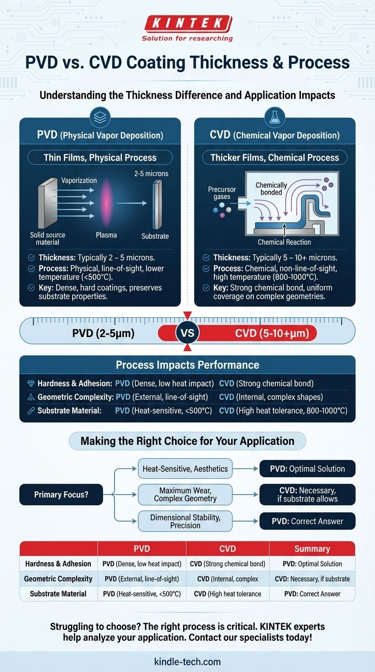
As a general rule, Physical Vapor Deposition (PVD) coatings are thinner than Chemical Vapor Deposition (CVD) coatings. PVD films typically measure between 2 and 5 microns, whereas CVD films are substantially thicker, usually ranging from 5 to 10 microns or more.
The difference in thickness is not an arbitrary choice; it is a direct result of the fundamental process used to create the coating. PVD physically deposits a thin layer, while CVD chemically grows a thicker one, and this distinction is the key to understanding which process is right for your application.
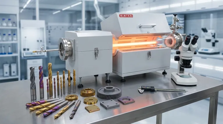
The Core Difference: Process Dictates Properties
The thickness of a coating is a direct consequence of its deposition method. PVD and CVD are entirely different processes at a molecular level, which explains the variation in their thickness, performance, and ideal use cases.
How PVD Works: Physical Deposition
PVD is a physical, line-of-sight process. In a vacuum chamber, a solid source material is vaporized into a plasma of atoms or molecules. These particles then travel in a straight line and condense onto the surface of the substrate, building a thin, dense film layer by layer.
The key attribute here is the lower process temperature. Because it doesn't rely on high heat to initiate a reaction, PVD can be used on a wider variety of materials, including those that are sensitive to heat.
How CVD Works: Chemical Reaction
CVD is a chemical process. Precursor gases are introduced into a chamber where they react on the surface of a heated substrate. This chemical reaction "grows" a new material directly on the part, forming a coating that is chemically bonded to the surface.
This method is not limited by line-of-sight, allowing the gases to flow around and inside complex parts for a highly uniform coating. The high temperatures required, however, are a critical limiting factor.
How Thickness and Process Impact Performance
Choosing between PVD and CVD is about more than just a few microns. It's about matching the process characteristics to your engineering goal.
Hardness and Adhesion
While thicker coatings like CVD are often associated with superior wear resistance, the reality is more nuanced. CVD's high-temperature process can create an exceptionally strong chemical bond (diffusion layer) with the substrate.
PVD coatings, though thinner, are often extremely dense and hard. Their lower deposition temperature also avoids altering the hardness or internal structure of the substrate material, which is a major advantage for precision tools.
Geometric Complexity
CVD excels at coating complex shapes. Because the deposition happens via a flowing gas, it can uniformly coat internal channels, sharp corners, and intricate geometries.
PVD’s line-of-sight nature makes it ideal for external surfaces but struggles with coating deep recesses or internal bores without complex part rotation and fixturing.
Substrate Material
This is often the deciding factor. The high heat of the CVD process (often 800-1000°C) will anneal, soften, or distort many steel tools and other heat-sensitive materials.
PVD's much lower process temperature (typically below 500°C) makes it the only viable option for parts that cannot tolerate thermal distortion.
Understanding the Trade-offs
Neither process is universally superior. Your choice depends on a clear understanding of their inherent compromises.
The PVD Compromise: Thinner Films and Line-of-Sight
PVD coatings are generally thinner and may offer less of a protective buffer in extremely high-wear applications compared to thick CVD. Furthermore, its line-of-sight deposition requires careful part orientation to ensure even coverage.
The CVD Compromise: High Heat and Environmental Impact
The primary drawback of CVD is its high process temperature, which significantly limits the range of compatible substrate materials. The process also involves volatile chemical precursors and creates hazardous byproducts that require careful handling and disposal, making it less environmentally friendly than PVD.
Appearance and Versatility
PVD offers a vast range of aesthetic options. It can be used to create coatings that are transparent, reflective, or a specific color. CVD coatings, by contrast, are typically opaque and offer very limited control over appearance.
Making the Right Choice for Your Application
Selecting the correct coating requires balancing the needs of the part with the capabilities of the process.
- If your primary focus is coating heat-sensitive materials or achieving specific optical properties: PVD is the superior choice due to its lower process temperatures and decorative versatility.
- If your primary focus is maximum wear resistance on a tough substrate or coating complex internal geometries: CVD is often the necessary solution, provided your part can withstand the high heat.
- If your primary focus is on dimensional stability for a precision component: PVD is almost always the correct answer, as it will not warp or change the substrate's core properties.
Ultimately, understanding that thickness is a consequence of the underlying process—physical deposition versus chemical reaction—is the key to selecting the right coating for your engineering goal.
Summary Table:
| Coating Type | Typical Thickness | Key Process Characteristic |
|---|---|---|
| PVD | 2 - 5 microns | Physical, line-of-sight, lower temperature (< 500°C) |
| CVD | 5 - 10+ microns | Chemical reaction, non-line-of-sight, high temperature (800-1000°C) |
Struggling to choose between a PVD or CVD coating for your components? The right coating process is critical for performance, durability, and cost-efficiency. KINTEK specializes in precision lab equipment and consumables for surface engineering. Our experts can help you analyze your application—whether it's for heat-sensitive tools, complex geometries, or maximum wear resistance—and recommend the optimal solution.
Contact our coating specialists today to discuss your project requirements and ensure you select the perfect coating for your success.
Visual Guide
Related Products
- Chemical Vapor Deposition CVD Equipment System Chamber Slide PECVD Tube Furnace with Liquid Gasifier PECVD Machine
- RF PECVD System Radio Frequency Plasma-Enhanced Chemical Vapor Deposition RF PECVD
- Customer Made Versatile CVD Tube Furnace Chemical Vapor Deposition Chamber System Equipment
- Split Chamber CVD Tube Furnace with Vacuum Station Chemical Vapor Deposition System Equipment Machine
- 1200℃ Split Tube Furnace with Quartz Tube Laboratory Tubular Furnace
People Also Ask
- What are the examples of CVD method? Discover the Versatile Applications of Chemical Vapor Deposition
- How are PECVD and CVD different? A Guide to Choosing the Right Thin-Film Deposition Process
- What is the difference between thermal CVD and PECVD? Choose the Right Thin-Film Deposition Method
- How plasma is generated in PECVD? A Step-by-Step Breakdown of the Process
- What is the precursor gas in PECVD? The Key to Low-Temperature Thin Film Deposition
