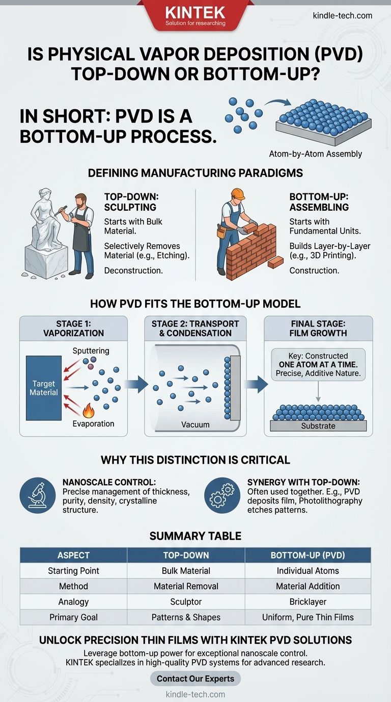
In short, Physical Vapor Deposition (PVD) is a bottom-up process. It operates by assembling a material layer-by-layer from its fundamental atomic or molecular components, rather than carving a structure out of a larger block of material.
The core distinction is one of construction versus deconstruction. PVD is a method of construction, building a thin film from the ground up, atom by atom, which places it squarely in the bottom-up manufacturing category.
Defining the Manufacturing Paradigms
To understand why PVD is a bottom-up technique, we first need to clearly define both manufacturing approaches. The difference is analogous to the distinction between a sculptor and a bricklayer.
The "Top-Down" Approach: Sculpting
The top-down approach begins with a large piece of bulk material, often called a substrate or wafer.
Material is then selectively removed through processes like etching or milling to create the desired shape and structure. Think of a sculptor carving a statue from a block of marble.
Photolithography is the classic example of a top-down process in microfabrication, where patterns are defined and unwanted material is etched away.
The "Bottom-Up" Approach: Assembling
The bottom-up approach, also known as additive manufacturing, starts with nothing and builds a structure from its constituent parts, such as atoms or molecules.
This is like a bricklayer building a wall one brick at a time or a 3D printer creating an object layer by layer. The final structure is assembled from its most basic units.
How PVD Fits the Bottom-Up Model
The mechanism of Physical Vapor Deposition aligns perfectly with the bottom-up philosophy of atomic-level assembly.
The PVD Mechanism
The PVD process has two primary stages, regardless of the specific technique (e.g., sputtering or thermal evaporation).
First, a solid source material (the "target") is converted into a vapor phase. This is done by bombarding it with ions (sputtering) or by heating it until it evaporates (evaporation).
Second, these vaporized atoms or molecules travel through a vacuum chamber and condense onto the surface of a substrate, gradually forming a thin, solid film.
Building from the Atom Up
The key is that the film is constructed one atom or molecule at a time. The process does not start with a larger block and remove material.
Instead, it begins with individual particles and assembles them into the desired thin-film structure. This methodical, additive nature is the very definition of a bottom-up process.
Why This Distinction Is Critical
Understanding PVD as a bottom-up technique is not just an academic classification; it has direct implications for its applications and limitations.
Control at the Nanoscale
Bottom-up processes like PVD offer exceptional control over the film's properties at the atomic level.
Because you are building the material from scratch, you can precisely manage its thickness, purity, density, and even its crystalline structure. This is crucial for creating high-performance optical coatings, semiconductors, and wear-resistant surfaces.
Synergy with Top-Down Methods
In practice, advanced manufacturing rarely uses one approach exclusively. Bottom-up and top-down methods are often used in sequence.
A typical workflow in the semiconductor industry involves first using a bottom-up process like PVD to deposit a perfectly uniform thin film of metal across a silicon wafer.
Then, a top-down process like photolithography is used to etch away parts of that metal film, creating the microscopic circuits and interconnects required for a processor.
Making the Right Choice for Your Goal
The choice between manufacturing approaches depends entirely on your end goal.
- If your primary focus is creating a pure, uniform, and extremely thin coating: A bottom-up process like PVD is the correct and often only choice.
- If your primary focus is creating complex, microscopic patterns on a surface: You will likely use PVD (bottom-up) to deposit the film and then photolithography (top-down) to create the pattern.
- If your primary focus is shaping a large, bulk piece of metal: Neither of these nanoscale techniques is appropriate; traditional top-down methods like machining or CNC milling are the standard.
Ultimately, classifying PVD as a bottom-up process provides a clear framework for understanding its fundamental strengths in building materials with precision from the smallest possible scale.
Summary Table:
| Aspect | Top-Down Process | Bottom-Up Process (PVD) |
|---|---|---|
| Starting Point | Bulk material (e.g., silicon wafer) | Individual atoms/molecules (vapor phase) |
| Method | Material removal (etching, milling) | Material addition (atom-by-atom condensation) |
| Analogy | Sculptor carving a statue | Bricklayer building a wall |
| Primary Goal | Creating patterns and shapes | Creating uniform, pure thin films |
Unlock Precision Thin Films with KINTEK PVD Solutions
Understanding that PVD is a bottom-up process is the first step to leveraging its power for your projects. This method is essential for applications requiring exceptional control over film thickness, purity, and structure at the nanoscale.
KINTEK specializes in high-quality lab equipment and consumables, including reliable PVD systems. Whether you are developing advanced semiconductors, durable protective coatings, or cutting-edge optical films, our expertise can help you achieve superior results.
Contact us today to discuss how our PVD solutions can enhance your research and production capabilities. Let's build the future of materials, one atom at a time.
Visual Guide
Related Products
- Chemical Vapor Deposition CVD Equipment System Chamber Slide PECVD Tube Furnace with Liquid Gasifier PECVD Machine
- RF PECVD System Radio Frequency Plasma-Enhanced Chemical Vapor Deposition RF PECVD
- Customer Made Versatile CVD Tube Furnace Chemical Vapor Deposition Chamber System Equipment
- Microwave Plasma Chemical Vapor Deposition MPCVD Machine System Reactor for Lab and Diamond Growth
- Custom CVD Diamond Coating for Lab Applications
People Also Ask
- What are the advantages of chemical vapor deposition? Achieve Superior Thin Films for Your Lab
- What is the chemical vapor deposition growth process? Build Superior Thin Films from the Atom Up
- What happens during deposition chemistry? Building Thin Films from Gaseous Precursors
- What are the processes of vapor phase deposition? Understand CVD vs. PVD for Superior Thin Films
- What is plasma enhanced chemical vapor deposition PECVD equipment? A Guide to Low-Temperature Thin Film Deposition


