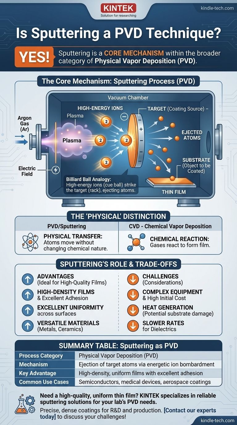
Yes, sputtering is a core technique within the broader category of Physical Vapor Deposition (PVD). Sputtering is not a separate process, but rather a specific mechanism used to achieve PVD. It works by using high-energy ions, typically from a noble gas like argon, to physically knock atoms off a target material, which then travel through a vacuum and deposit onto a substrate as a thin film.
The critical distinction is that Physical Vapor Deposition (PVD) is the category of coating processes that transfer material physically, while sputtering is a specific method within that category that uses particle bombardment to vaporize the material.
How Sputtering Works as a PVD Process
To understand the relationship fully, it's essential to break down the sputtering mechanism itself. The entire process is fundamentally a physical one, which is why it falls under the PVD umbrella.
The Core Mechanism: A Billiard Ball Analogy
At its heart, sputtering involves the ejection of atoms from a solid target material. Imagine a cue ball striking a tightly packed rack of billiard balls; the energy transfer causes balls to fly off. In sputtering, high-energy ions are the "cue ball," and the target material is the "rack."
Creating the Sputtering Environment
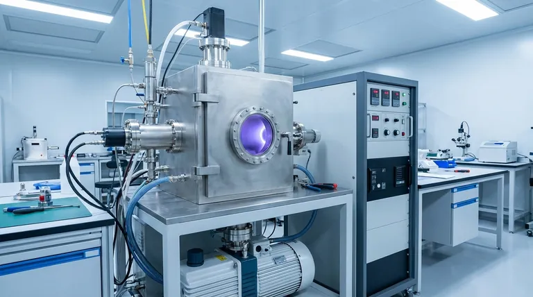
The process begins by introducing an inert gas, almost always argon, into a vacuum chamber. An electric field is applied, which ignites the gas into a plasma—a cloud of energized ions and electrons.
Bombardment and Deposition
The target material (the coating source) is given a negative electrical charge. This causes the positive argon ions from the plasma to accelerate and collide violently with the target surface. These collisions have enough energy to dislodge or "sputter" atoms from the target.
These freed atoms then travel through the vacuum chamber and condense on the substrate (the object being coated), gradually building up a thin, uniform film.
The "Physical" Distinction
A key reason sputtering is a PVD technique is the absence of a chemical reaction. The atoms are moved from the target to the substrate without changing their chemical nature. This stands in contrast to Chemical Vapor Deposition (CVD), where gases react to form the film on the substrate surface.
Sputtering's Role in the PVD Family
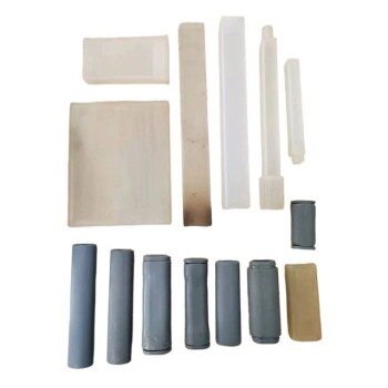
Sputtering is one of the most common and versatile PVD methods used in industries ranging from semiconductor manufacturing to medical devices and aerospace.
A Highly Controllable Process
The quality and properties of the final film are heavily influenced by process parameters. Controlling factors like the sputtering gas pressure and the sputtering rate (how many atoms are ejected over time) allows for precise control over the film's thickness, density, and structure.
Common Sputtering Variations
The basic sputtering technique has been enhanced over time. You will often encounter terms like magnetron sputtering, which uses powerful magnets to trap electrons near the target, increasing the efficiency of the plasma and allowing for higher deposition rates.
Understanding the Trade-offs
Like any engineering process, sputtering has distinct advantages and disadvantages that make it suitable for some applications but less ideal for others.
The Advantages of Sputtering
Sputtering is renowned for its ability to produce very high-density films with excellent adhesion. The process offers high throughput and can create coatings with excellent uniformity across a wide surface area. It is also compatible with a vast multitude of materials, including metals and ceramics.
The Limitations and Challenges
The equipment for sputtering can be complex and carry a high initial cost. The process can also generate significant heat, which may damage sensitive substrates. Furthermore, sputtering certain materials, particularly dielectrics (electrical insulators), can have poor deposition rates compared to other methods.
Making the Right Choice for Your Application
Ultimately, choosing a deposition technique depends entirely on your project's goals and constraints.
- If your primary focus is creating high-quality, dense, and uniform films from a wide variety of materials: Sputtering is a powerful and reliable PVD method to consider.
- If your primary focus is depositing on heat-sensitive substrates or keeping initial equipment costs low: You may need to evaluate the limitations of sputtering and explore alternative techniques.
By understanding sputtering as a fundamental PVD mechanism, you can better determine its suitability for your specific material science and engineering challenges.
Summary Table:
| Aspect | Detail |
|---|---|
| Process Category | Physical Vapor Deposition (PVD) |
| Mechanism | Ejection of target atoms via energetic ion bombardment |
| Key Advantage | High-density, uniform films with excellent adhesion |
| Common Use Cases | Semiconductors, medical devices, aerospace coatings |
Need a high-quality, uniform thin film for your project? KINTEK specializes in lab equipment and consumables, providing reliable sputtering solutions for your laboratory's PVD needs. Our expertise ensures you achieve precise, dense coatings for applications in R&D and production. Contact our experts today to discuss how we can support your specific material science challenges!
Visual Guide
Related Products
- Inclined Rotary Plasma Enhanced Chemical Vapor Deposition PECVD Equipment Tube Furnace Machine
- 915MHz MPCVD Diamond Machine Microwave Plasma Chemical Vapor Deposition System Reactor
- HFCVD Machine System Equipment for Drawing Die Nano-Diamond Coating
- Laboratory Sterilizer Lab Autoclave Pulse Vacuum Lifting Sterilizer
- CVD Diamond Cutting Tool Blanks for Precision Machining
People Also Ask
- What is plasma in CVD process? Lowering Deposition Temperatures for Heat-Sensitive Materials
- What is plasma enhanced chemical vapor deposition? Achieve Low-Temperature, High-Quality Thin Films
- How does plasma enhanced CVD work? Achieve Low-Temperature, High-Quality Thin Film Deposition
- What is the difference between CVD and PECVD? Choose the Right Thin-Film Deposition Method
- What is meant by vapor deposition? A Guide to Atomic-Level Coating Technology