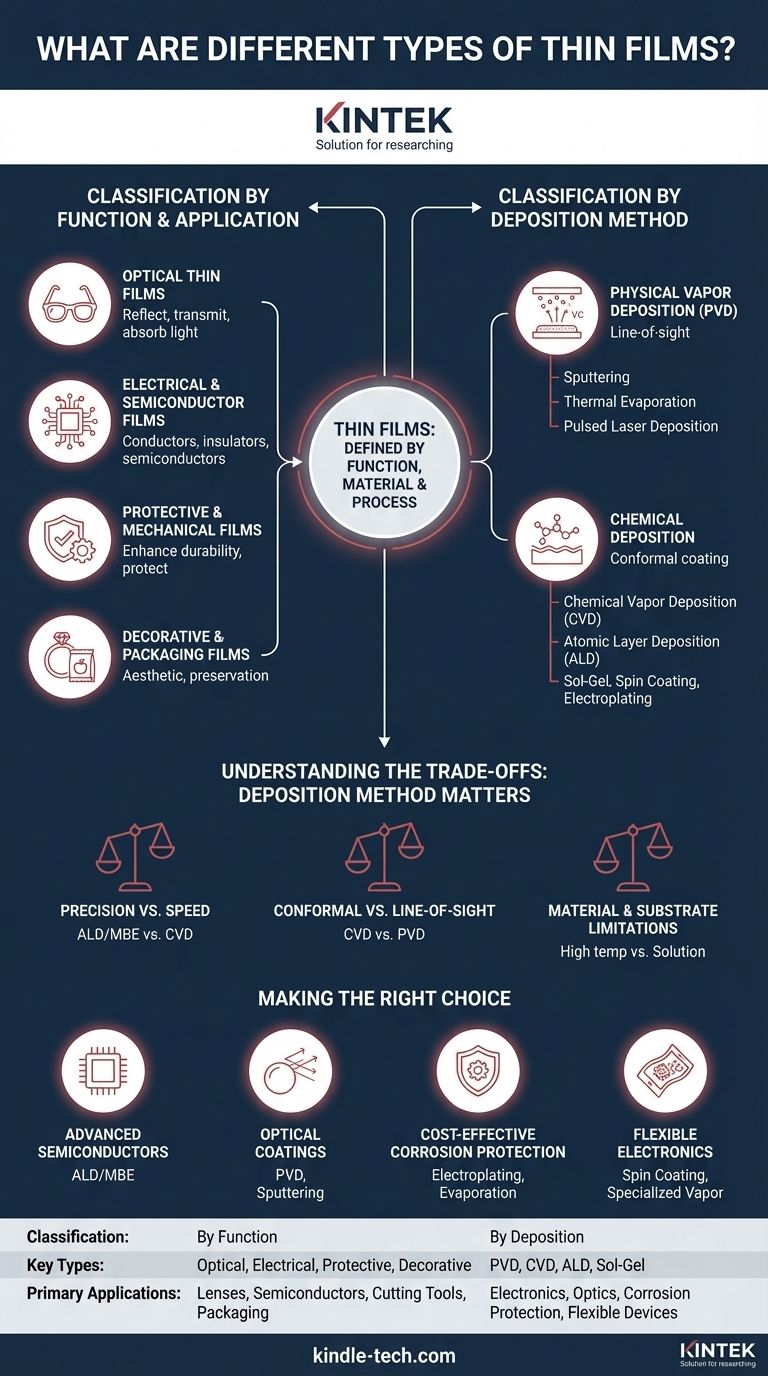
A thin film is primarily categorized by either its function or its manufacturing method. Functionally, films are broadly grouped into optical films that manipulate light and electrical films that manage current. More fundamentally, they are classified by their deposition process, which falls into two main families: Chemical Deposition and Physical Deposition, each containing numerous specific techniques.
The most effective way to understand thin films is not by memorizing a list of types, but by recognizing that a film is defined by the intersection of its application (what it does), its material (what it's made of), and its deposition method (how it's made).
Classification by Function and Application
The most intuitive way to classify thin films is by their end-use. This approach focuses on the problem the film is designed to solve.
Optical Thin Films
These films are engineered to interact with light. Their primary purpose is to reflect, transmit, or absorb specific wavelengths.
Common examples include anti-reflective coatings on eyeglasses, mirror coatings on telescope optics, and light-filtering layers in solar cells and architectural glass.
Electrical and Semiconductor Films
These films form the building blocks of modern electronics. They can be designed as conductors, insulators, or semiconductors.
They are indispensable in integrated circuits, LEDs, touch-screen displays, and thin-film transistors that power everything from monitors to flexible electronics.
Protective and Mechanical Films
This category focuses on enhancing a substrate's durability. The goal is to protect against environmental or physical damage.
These include hard, wear-resistant coatings on cutting tools, anti-corrosion layers on metal parts, and scratch-resistant films on consumer products.
Decorative and Packaging Films
While often functional, these films have a primary aesthetic or consumer purpose.
Applications range from the thin layers of gold on jewelry to the metallic films in food packaging that preserve freshness and provide a reflective barrier.
Classification by Deposition Method
A more technical and fundamental classification is based on how the film is created. The choice of method dictates the film's purity, uniformity, thickness control, and cost. All methods fall under two primary umbrellas.
Physical Vapor Deposition (PVD)
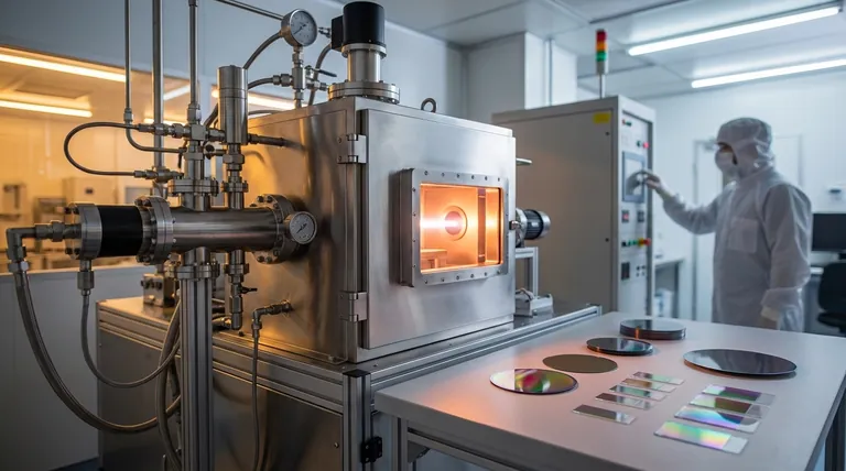
PVD involves mechanically or thermally turning a solid source material into a vapor, which then condenses onto the substrate surface in a vacuum. It is a "line-of-sight" process.
Key PVD methods include Sputtering, Thermal Evaporation, and Pulsed Laser Deposition (PLD). These are widely used for metals, alloys, and certain ceramic coatings.
Chemical Deposition
These methods use chemical reactions to form the film. They are generally better at coating complex, non-flat surfaces conformally.
The most prominent method is Chemical Vapor Deposition (CVD), where precursor gases react on a heated substrate. Other important methods include Atomic Layer Deposition (ALD) for ultra-precise, atom-by-atom layers, and liquid-phase methods like Sol-Gel, Spin Coating, and Electroplating.
Understanding the Trade-offs: Deposition Method Matters
The selection of a deposition method is a critical engineering decision driven by a series of trade-offs between performance, cost, and material compatibility.
Precision vs. Speed
Methods like Atomic Layer Deposition (ALD) and Molecular Beam Epitaxy (MBE) offer unparalleled, atomic-level control over thickness and composition. This precision is essential for advanced semiconductors but comes at the cost of being extremely slow and expensive.
Conformal vs. Line-of-Sight
CVD methods excel at creating uniform coatings over complex, 3D structures because the precursor gases can reach all surfaces. PVD methods are line-of-sight, making them ideal for flat surfaces but challenging for coating intricate shapes without complex substrate manipulation.
Material and Substrate Limitations
Some materials can only be deposited by specific methods. Furthermore, some deposition techniques require very high temperatures, which can damage sensitive substrates like polymers or certain electronic components. Wet chemical methods like spin coating are only suitable for materials that can be put into a liquid solution.
Making the Right Choice for Your Goal
The "best" type of thin film is entirely dependent on the specific engineering or scientific goal.
- If your primary focus is advanced semiconductor performance: You will work with films created by highly precise methods like ALD or MBE to achieve atomic-level control over layer thickness and purity.
- If your primary focus is optical coatings on lenses or glass: Your concern will be materials with specific refractive indices, often applied via PVD methods like sputtering for high uniformity and quality.
- If your primary focus is cost-effective corrosion protection on a large part: You might look toward scalable chemical methods like electroplating or physical methods like thermal evaporation.
- If your primary focus is flexible electronics or organic LEDs (OLEDs): You will be exploring polymer-based films applied with methods like spin coating or specialized vapor deposition techniques.
Ultimately, understanding a thin film means seeing it not as a single "type," but as a solution engineered at the intersection of function, material, and process.
Summary Table:
| Classification | Key Types | Primary Applications |
|---|---|---|
| By Function | Optical, Electrical, Protective, Decorative | Lenses, Semiconductors, Cutting Tools, Packaging |
| By Deposition | PVD (Sputtering, Evaporation), CVD, ALD, Sol-Gel | Electronics, Optics, Corrosion Protection, Flexible Devices |
Need expert guidance on selecting the right thin film solution for your project? At KINTEK, we specialize in lab equipment and consumables for thin film deposition, serving a wide range of laboratory needs. Whether you're developing advanced semiconductors, optical coatings, or protective layers, our expertise can help you optimize your process for performance, cost, and material compatibility. Contact us today to discuss how we can support your research and production goals!
Visual Guide
Related Products
- Tungsten Evaporation Boat for Thin Film Deposition
- Aluminum-Plastic Flexible Packaging Film for Lithium Battery Packaging
- Thin-Layer Spectral Electrolysis Electrochemical Cell
- Lab Plastic PVC Calender Stretch Film Casting Machine for Film Testing
People Also Ask
- What is the layer method of deposition? A Guide to PVD vs. CVD Thin-Film Techniques
- What is the method of deposition of thin films? Choose the Right PVD or CVD Technique for Your Lab
- What is the process of thin film deposition? A Guide to PVD, CVD, and Coating Techniques
- What methods are used to deposit thin films? A Guide to PVD, CVD, and ALD Techniques
- What are the types of thin film? A Guide to PVD vs. CVD Deposition Methods


