At its core, a sputtering system is a sophisticated tool for depositing ultra-thin films of material onto a surface. This process, a type of Physical Vapor Deposition (PVD), allows for the creation of precise coatings that can fundamentally alter the properties of an object, making it a cornerstone technology in industries ranging from semiconductors and aerospace to medical devices and architectural design.
Sputtering is not merely about applying a layer; it's about engineering a surface at the atomic level. This technique enables us to make materials more durable, electrically conductive, corrosion-resistant, or optically unique, solving critical challenges across countless high-tech fields.
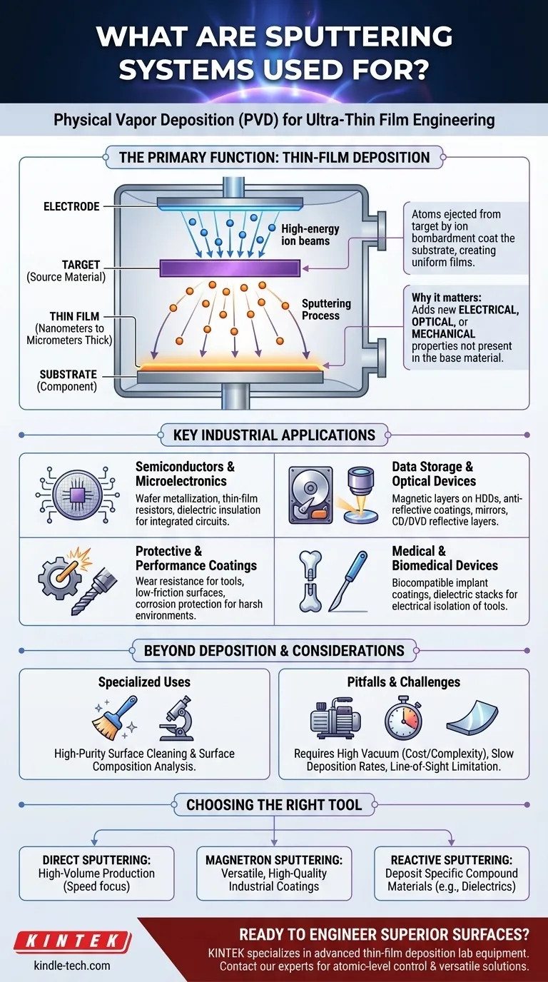
The Primary Function: Thin-Film Deposition
Sputtering's main purpose is to create high-performance coatings, known as thin films. These layers can be anywhere from a few nanometers to several micrometers thick.
What is Sputter Deposition?
The process takes place in a high-vacuum chamber. High-energy ions are used to bombard a source material, known as the target.
This bombardment ejects or "sputters" atoms from the target. These atoms then travel through the vacuum and deposit onto a component, called the substrate, forming a thin, highly uniform film.
Why Are These Films Important?
These engineered films are not just protective layers; they add entirely new functionalities to the substrate's surface.
The goal is to impart specific electrical, optical, or mechanical properties that the underlying material does not possess on its own.
Key Industrial Applications of Sputtering
The ability to precisely control surface properties has made sputtering indispensable across many sectors. The specific type of sputtering system—such as direct, magnetron, or reactive—is chosen based on the desired outcome.
Semiconductors and Microelectronics
This is arguably the largest application for sputtering. It is critical for building the complex, layered structures of integrated circuits.
Uses include wafer metallization (depositing conductive layers), creating thin-film resistors from materials like tantalum nitride, and depositing dielectric films for insulation.
Data Storage and Optical Devices
Sputtering is used to create the magnetic layers on hard disk drives and the reflective layers on CDs and DVDs.
For optical components, it is used to apply anti-reflective coatings to lenses, create specialized filters, and produce highly reflective mirror surfaces.
Protective and Performance Coatings
For industrial, automotive, and aerospace components, performance is paramount. Sputtering delivers robust coatings that enhance durability.
These include wear-resistant coatings for cutting tools, low-friction coatings for moving parts, and corrosion-resistant films to protect materials in harsh environments.
Medical and Biomedical Devices
In the medical field, surface properties can be a matter of life and death. Sputtering provides biocompatible coatings for implants.
It is also used to create dielectric stacks that electrically isolate surgical tools, ensuring patient safety during delicate procedures.
Sputtering Beyond Film Deposition
While deposition is its primary use, the fundamental sputtering process has other specialized applications in research and quality control.
High-Purity Surface Cleaning
Before a deposition process begins, the sputtering mechanism can be used to clean a substrate's surface.
The ion bombardment effectively etches away contaminants at an atomic level, preparing an ultra-pure surface that is ready for coating.
Surface Composition Analysis
By analyzing the material that is sputtered off a target, scientists can determine the precise chemical composition of its surface. This is a powerful analytical technique in materials science.
Common Pitfalls and Considerations
While powerful, sputtering is a complex process with specific requirements that dictate its use. Understanding these trade-offs is key to its successful application.
Requirement for High Vacuum
Sputtering systems are not simple machines. They require a high-vacuum environment to ensure the sputtered atoms can travel from the target to the substrate without colliding with air molecules.
This requirement adds significant cost, complexity, and processing time compared to atmospheric coating methods.
Deposition Rate Limitations
While effective, sputtering can be a relatively slow process. The choice between systems like direct sputtering for high-volume production and other methods often comes down to a trade-off between deposition speed and film quality.
Line-of-Sight Deposition
In many sputtering configurations, the deposition is "line-of-sight," meaning the target material can only coat surfaces it can directly "see."
This can make it challenging to uniformly coat complex, three-dimensional shapes without sophisticated substrate manipulation and rotation systems.
Making the Right Choice for Your Goal
The specific sputtering technique used is directly tied to the final application and the type of material being deposited.
- If your primary focus is high-volume production and speed: Direct sputtering systems are engineered for maximum deposition rates, essential for semiconductor and flat-panel display manufacturing.
- If your primary focus is versatile, high-quality industrial coatings: Magnetron sputtering is the standard for creating wear-resistant, decorative, or optically specific films on a wide range of products.
- If your primary focus is depositing specific compound materials: Reactive sputtering, which introduces a gas like nitrogen or oxygen, is necessary for creating films like dielectrics or specific semiconductors.
Ultimately, sputtering provides precise, atomic-level control over a material's surface, making it an indispensable tool for modern engineering.
Summary Table:
| Application Area | Key Uses of Sputtering |
|---|---|
| Semiconductors | Wafer metallization, thin-film resistors, dielectric insulation |
| Optics & Data Storage | Anti-reflective coatings, reflective layers for CDs/DVDs, magnetic films for HDDs |
| Protective Coatings | Wear resistance, corrosion protection, low-friction surfaces |
| Medical Devices | Biocompatible implant coatings, dielectric insulation for surgical tools |
Ready to Engineer Superior Surfaces with Precision Sputtering?
Whether you're developing next-generation semiconductors, durable industrial components, or life-saving medical devices, the right sputtering system is critical to your success. KINTEK specializes in advanced lab equipment and consumables for thin-film deposition, serving the precise needs of research and production laboratories.
We provide solutions that deliver:
- Atomic-level control for unmatched film uniformity and quality
- Versatile configurations (magnetron, reactive, direct) tailored to your specific material and application goals
- Enhanced performance for your substrates, from conductivity and durability to optical properties
Let's discuss your project requirements. Contact our experts today to find the ideal sputtering solution for your laboratory's challenges.
Visual Guide
Related Products
- Spark Plasma Sintering Furnace SPS Furnace
- Vacuum Induction Melting Spinning System Arc Melting Furnace
- Chemical Vapor Deposition CVD Equipment System Chamber Slide PECVD Tube Furnace with Liquid Gasifier PECVD Machine
- Customer Made Versatile CVD Tube Furnace Chemical Vapor Deposition Chamber System Equipment
People Also Ask
- What is the mechanism of SPS process? A Deep Dive into Rapid, Low-Temperature Sintering
- What is the difference between spark plasma sintering and flash sintering? A Guide to Advanced Sintering Methods
- What is the process fundamentals of spark plasma sintering? Achieve Rapid, High-Density Material Consolidation
- What technical advantages does a Spark Plasma Sintering (SPS) furnace offer for LZP ceramics? Enhance Ionic Conductivity
- What is the theory of spark plasma sintering? A Guide to Rapid, Low-Temperature Densification


