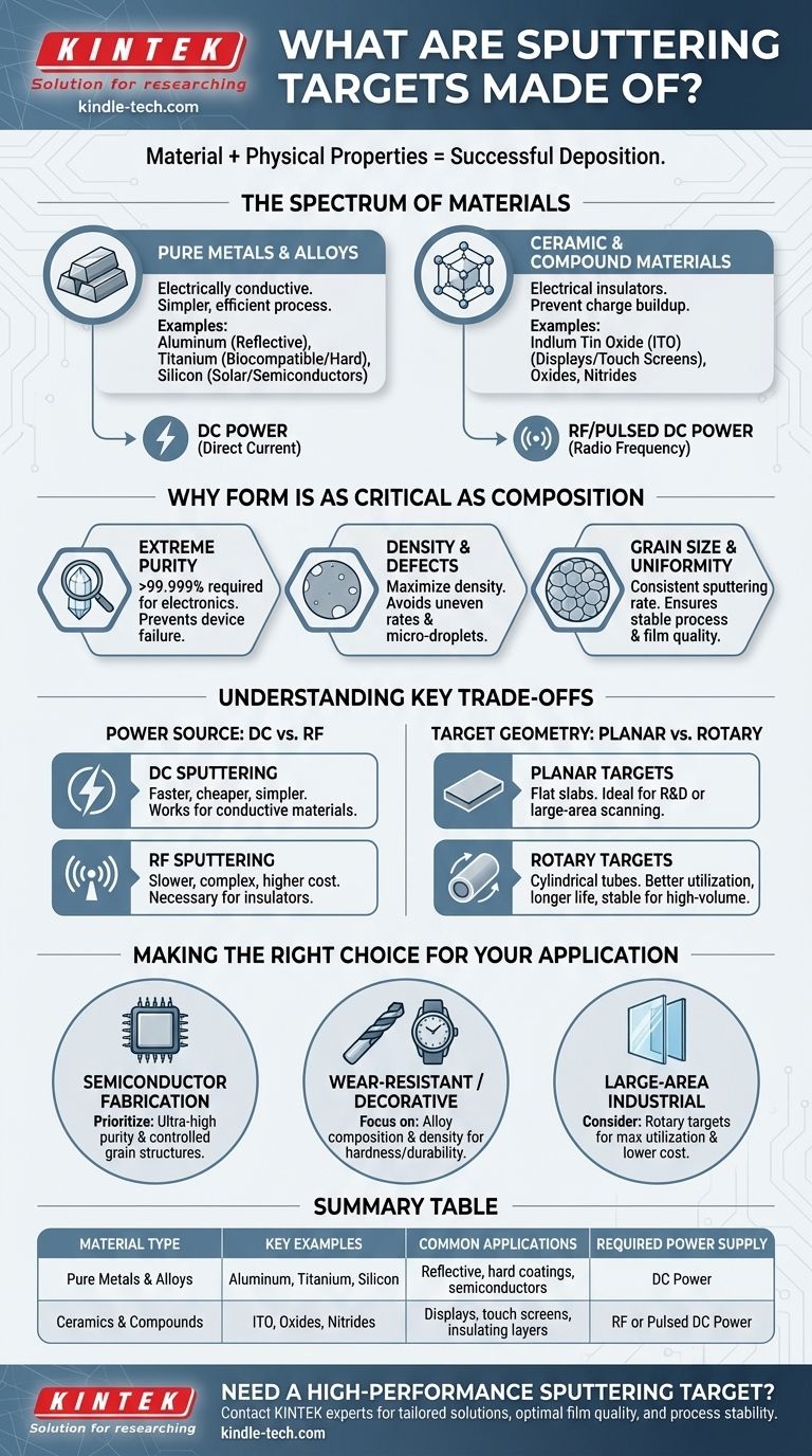
At their core, sputtering targets are made of the exact material you intend to deposit as a thin film. This includes a vast range of materials, from pure metals like silicon and titanium to complex alloys and ceramic compounds like oxides or nitrides. The choice of material is dictated entirely by the desired properties of the final coating.
The material a sputtering target is made of only tells half the story. The true determinant of a successful deposition process lies in the target's physical and structural properties—its purity, density, and uniformity are just as critical as its chemical composition.
The Spectrum of Sputtering Target Materials
Sputtering is a highly versatile process with few restrictions on source material. The targets are categorized based on their composition and electrical conductivity, which directly influences the type of power supply required for the deposition process.
Pure Metals and Alloys
The most straightforward targets are made from a single metallic element or a pre-defined alloy. These materials are electrically conductive, which allows for a simpler and more efficient deposition process using a Direct Current (DC) power supply.
Common examples include aluminum for reflective coatings, titanium for biocompatible or hard coatings, and silicon for manufacturing solar cells and semiconductors.
Ceramic and Compound Materials
This category includes materials that are often electrical insulators, such as oxides and nitrides. A prominent example is Indium Tin Oxide (ITO), a transparent conductive oxide essential for manufacturing displays and touch screens.
Because these materials do not conduct electricity well, they require a Radio Frequency (RF) or pulsed DC power supply to prevent charge buildup on the target surface, which would otherwise halt the sputtering process.
Why Form Is as Critical as Composition
A sputtering target is far more than a simple block of material. It is a highly engineered component where physical characteristics are meticulously controlled to ensure a stable and repeatable deposition process. The quality of the target directly translates to the quality of the final thin film.
The Requirement for Extreme Purity
In applications like integrated circuits, even minuscule impurities in the target can be sputtered onto the substrate, altering the film's electrical properties and causing device failure. Therefore, targets for electronics are often required to have purities exceeding 99.999%.
The Impact of Density and Defects
A target must be as dense as possible, often approaching its theoretical maximum density. Voids or defects within the target can lead to uneven sputtering rates and the ejection of undesirable micro-droplets, which create defects in the deposited film. Fabrication methods like Cold Isostatic Pressing (CIP) followed by sintering are used to create dense, stable ceramic targets.
The Role of Grain Size and Uniformity
A uniform, fine-grained microstructure across the target is essential for achieving a consistent sputtering rate. Large or non-uniform grains can erode at different speeds, causing instability in the process and variations in the final film's thickness and composition.
Understanding the Key Trade-offs
Choosing a target involves balancing material properties, process requirements, and cost. Two fundamental decisions involve the power source and the target's physical geometry.
Power Source: DC vs. RF
The choice between DC and RF power is dictated by the target material. DC sputtering is faster, cheaper, and simpler, but it only works for conductive materials like metals and some alloys.
RF sputtering is more complex and generally slower, but it is the necessary choice for depositing insulating materials like oxides and nitrides. This versatility comes at a higher equipment and operational cost.
Target Geometry: Planar vs. Rotary
Targets come in different shapes, with planar and rotary being the most common. Planar targets are flat, rectangular, or circular slabs ideal for R&D systems or large-area linear scanning processes, like coating architectural glass.
Rotary (or rotatable) targets are cylindrical tubes that rotate during sputtering. They offer better material utilization, longer operational lifetimes, and more stable process control, making them a preferred choice for high-volume manufacturing environments.
Making the Right Choice for Your Application
The ideal sputtering target depends entirely on your end goal, balancing the performance requirements of your film against the practicalities of the deposition process.
- If your primary focus is semiconductor fabrication: Prioritize ultra-high purity targets and materials with controlled grain structures to guarantee the electrical integrity of your thin films.
- If your primary focus is wear-resistant or decorative coatings: Focus on the target's alloy composition and density to achieve the desired hardness, durability, and final appearance.
- If your primary focus is large-area industrial coating: Consider rotary targets to maximize material utilization, increase uptime, and lower the overall cost per unit.
Ultimately, selecting the right sputtering target is a critical decision that directly influences the quality, performance, and cost of your final product.
Summary Table:
| Material Type | Key Examples | Common Applications | Required Power Supply |
|---|---|---|---|
| Pure Metals & Alloys | Aluminum, Titanium, Silicon | Reflective coatings, hard coatings, semiconductors | DC Power |
| Ceramics & Compounds | Indium Tin Oxide (ITO), Oxides, Nitrides | Displays, touch screens, insulating layers | RF or Pulsed DC Power |
Need a high-performance sputtering target for your specific application?
At KINTEK, we specialize in manufacturing premium lab equipment and consumables, including sputtering targets tailored to your exact needs. Whether you require ultra-high purity for semiconductor fabrication, durable alloys for wear-resistant coatings, or efficient rotary targets for large-scale production, our expertise ensures optimal film quality and process stability.
Let us help you achieve superior thin-film results. Contact our experts today to discuss your project requirements!
Visual Guide