At its core, Atomic Layer Deposition (ALD) provides unparalleled control over the growth of thin films. This technique enables the creation of perfectly uniform and conformal coatings with thickness controlled down to the single atomic layer. However, this level of precision is achieved through a slow, cyclical process, making it less suitable for applications that demand high-speed, high-volume production.
The fundamental trade-off of ALD is sacrificing manufacturing speed for ultimate control. It is the ideal choice for applications where film quality, uniformity, and conformity are non-negotiable, but a poor fit for high-volume, low-cost coating needs.
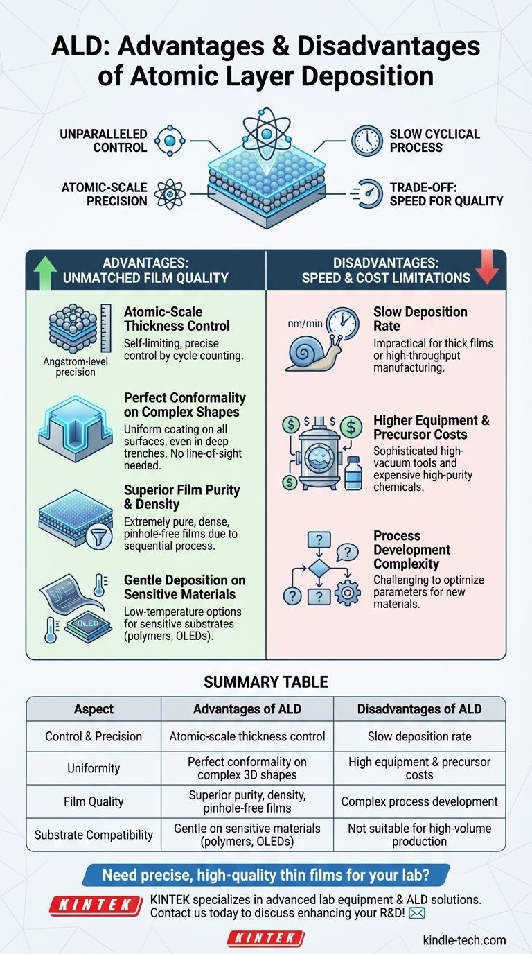
The Core Advantages: Unmatched Film Quality
ALD's unique layer-by-layer process gives it several distinct advantages over traditional deposition methods like Physical Vapor Deposition (PVD) or Chemical Vapor Deposition (CVD).
Atomic-Scale Thickness Control
The process is self-limiting. Each cycle of precursor and reactant exposure deposits exactly one monolayer, allowing you to control the final film thickness with angstrom-level precision simply by counting the number of cycles performed.
Perfect Conformality on Complex Shapes
ALD does not require a direct line-of-sight to the substrate. The gaseous precursors fill the entire chamber, coating every exposed surface evenly. This results in a film that is perfectly conformal over complex, three-dimensional topographies and high-aspect-ratio structures.
Superior Film Purity and Density
The sequential nature of the process, with purge steps in between each chemical exposure, ensures that excess precursors and reaction by-products are completely removed. This leads to extremely pure, dense, and pinhole-free films with excellent barrier properties.
Gentle Deposition on Sensitive Materials
ALD can be performed at a wide range of temperatures, including near room temperature. This, combined with low-power plasma options, makes it a gentle process suitable for coating sensitive substrates like polymers, flexible electronics, and organic devices (OLEDs) without causing damage.
Understanding the Trade-offs: Speed and Cost
The precision of ALD comes with significant practical limitations that must be considered.
The Primary Disadvantage: Slow Deposition Rate
The greatest drawback of ALD is its speed. Because the film is built one atomic layer at a time in a multi-step cycle, deposition rates are typically very low—often measured in angstroms or nanometers per minute. This makes it impractical for depositing thick films or for high-throughput manufacturing.
Higher Equipment and Precursor Costs
ALD systems are sophisticated high-vacuum tools that are generally more expensive than their PVD or CVD counterparts. Furthermore, the high-purity chemical precursors required for the process can also be costly and require specialized handling.
Process Development Complexity
While the concept is simple, developing a robust ALD process for a new material can be challenging. It requires careful research to find the right combination of precursors, temperature, and pulse/purge timings to achieve the desired self-limiting growth.
How to Apply This to Your Project
Choosing a deposition method depends entirely on your project's critical requirements. The unique characteristics of ALD make it the ideal solution for some of the most demanding applications in modern technology.
- If your primary focus is ultimate performance and precision: ALD is the superior choice for creating ultrathin, conformal, and pinhole-free films, especially for advanced microelectronics or high-performance optics.
- If your primary focus is high-volume manufacturing and cost-efficiency: You should evaluate faster methods like CVD or PVD, as ALD's slow deposition rate will likely be a bottleneck for thick films or large-area coatings.
- If your primary focus is coating complex 3D structures or sensitive materials: ALD's exceptional conformality and low-temperature capabilities make it uniquely suited for coating MEMS, medical implants, polymers, and other challenging substrates.
Ultimately, ALD is a tool of precision, best leveraged when the quality and conformity of the film cannot be compromised.
Summary Table:
| Aspect | Advantages of ALD | Disadvantages of ALD |
|---|---|---|
| Control & Precision | Atomic-scale thickness control | Slow deposition rate |
| Uniformity | Perfect conformality on complex 3D shapes | High equipment and precursor costs |
| Film Quality | Superior purity, density, and pinhole-free films | Complex process development |
| Substrate Compatibility | Gentle deposition on sensitive materials (e.g., polymers, OLEDs) | Not suitable for high-volume production |
Need precise, high-quality thin films for your lab? KINTEK specializes in providing advanced lab equipment and consumables, including ALD solutions, to help you achieve unparalleled film uniformity and conformity for your most demanding applications. Let our experts guide you to the right deposition technology for your specific needs. Contact us today to discuss how we can enhance your research and development process!
Visual Guide
Related Products
- RF PECVD System Radio Frequency Plasma-Enhanced Chemical Vapor Deposition RF PECVD
- Chemical Vapor Deposition CVD Equipment System Chamber Slide PECVD Tube Furnace with Liquid Gasifier PECVD Machine
- HFCVD Machine System Equipment for Drawing Die Nano-Diamond Coating
- 915MHz MPCVD Diamond Machine Microwave Plasma Chemical Vapor Deposition System Reactor
- Inclined Rotary Plasma Enhanced Chemical Vapor Deposition PECVD Equipment Tube Furnace Machine
People Also Ask
- What is plasma enhanced chemical vapour deposition PECVD used for? Enable Low-Temp Thin Films for Electronics & Solar
- How does plasma enhance CVD? Unlock Low-Temperature, High-Quality Film Deposition
- Why is a Matching Network Indispensable in RF-PECVD for Siloxane Films? Ensure Stable Plasma and Uniform Deposition
- What is plasma enhanced chemical Vapour deposition process used for fabrication of? A Guide to Low-Temperature Thin Films
- What is plasma chemical vapor deposition? A Low-Temperature Thin Film Coating Solution


