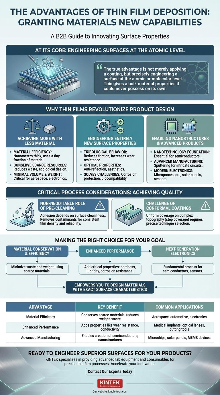
At its core, thin film deposition is a manufacturing process that grants materials new capabilities. It allows us to apply an incredibly thin, highly controlled layer of one material onto a substrate, fundamentally changing its surface properties. The primary advantages are the ability to conserve scarce materials, improve the functionality of existing products, reduce weight, and create entirely new technologies that would otherwise be impossible.
The true advantage of thin film deposition is not merely applying a coating, but precisely engineering a surface at the atomic or molecular level. This gives a bulk material properties—such as electrical conductivity, wear resistance, or optical characteristics—that it could never possess on its own.
Why Thin Films Revolutionize Product Design
Thin film deposition solves a fundamental engineering problem: the properties needed on the surface of an object are often different from the properties needed in its bulk structure. Deposition techniques allow designers to choose the best material for each role independently.
Achieving More with Less Material
A key benefit is material efficiency. By depositing a layer only a few nanometers or micrometers thick, you can achieve the desired surface property using a tiny fraction of the material required for a solid object.
This directly leads to the conservation of scarce or expensive materials. It also contributes to more ecological designs by reducing power consumption and effluent output compared to other coating methods.
Finally, this approach adds minimal volume and weight, which is a critical advantage in industries like aerospace, automotive, and portable electronics.
Engineering Entirely New Surface Properties
The core function of a thin film is to provide properties that the base material lacks. This allows for a massive upgrade in functionality.
Common enhancements include improving tribological behavior (reducing friction and increasing wear resistance), enhancing optical properties (like anti-reflection coatings on lenses), or improving aesthetics.
This process is how we solve long-standing engineering challenges, such as protecting components from corrosion or making medical implants biocompatible.
Enabling Nanostructures and Advanced Products
Thin film deposition is not just for improving existing products; it is essential for creating new ones. The precision of these techniques is fundamental to the nanotechnology sector.
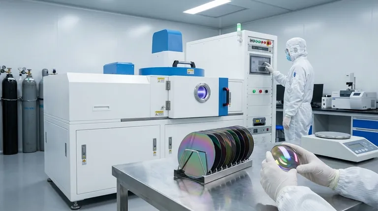
Processes like sputtering, where atoms are ejected from a target material onto a substrate, are the bedrock of the semiconductor industry. This is how the intricate, layered circuits on silicon wafers are built.
Without this technology, modern electronics, from microprocessors to solar panels, simply would not exist.
Understanding the Critical Process Considerations
While the advantages are significant, achieving them requires careful control over the deposition process. The quality of the outcome is not automatic and depends on several critical factors.
The Non-Negotiable Role of Pre-Cleaning
A thin film's performance is entirely dependent on its ability to adhere to the substrate. Any contaminants on the surface can cause the film to peel, blister, or fail.
Thorough pre-cleaning is therefore essential. It removes particles and residues, ensuring strong adhesion and consistent film density, which is vital for achieving the desired optical or electrical properties.
In high-volume manufacturing, effective pre-cleaning improves yield and reliability, ultimately lowering the total cost of ownership.
The Challenge of Conformal Coatings
When depositing a film onto a substrate with complex topography, such as a microchip with trenches, uniform coverage is a major challenge.
This is measured by fill capability, or step coverage. It represents how well the film covers the sidewalls and bottom of a feature compared to the top surface.
Achieving a high-quality, conformal coating that is uniform across an intricate surface requires selecting the right deposition technique and carefully tuning its parameters.
Making the Right Choice for Your Goal
The decision to use thin film deposition should be driven by a clear understanding of your primary objective.
- If your primary focus is material conservation and efficiency: This technology provides an unparalleled way to use scarce or expensive materials only where they are needed, minimizing waste and weight.
- If your primary focus is enhanced performance: Use deposition to add critical surface properties like hardness, lubricity, corrosion resistance, or specific optical characteristics to an otherwise standard component.
- If your primary focus is creating next-generation electronics: Thin film deposition is the fundamental fabrication process for semiconductors, sensors, and other advanced electronic devices.
Ultimately, thin film deposition empowers you to design materials with the exact surface characteristics your application demands.
Summary Table:
| Advantage | Key Benefit | Common Applications |
|---|---|---|
| Material Efficiency | Conserves scarce/expensive materials; reduces weight and waste. | Aerospace, automotive, electronics. |
| Enhanced Performance | Adds properties like wear resistance, conductivity, or biocompatibility. | Medical implants, optical lenses, cutting tools. |
| Advanced Manufacturing | Enables the creation of semiconductors, sensors, and nanostructures. | Microchips, solar panels, MEMS devices. |
Ready to engineer superior surfaces for your products?
Thin film deposition is the key to solving complex material challenges, from enhancing durability to enabling next-generation electronics. At KINTEK, we specialize in providing the advanced lab equipment and consumables necessary for precise and reliable thin film processes.
Whether you are developing new semiconductors, improving medical devices, or optimizing industrial components, our expertise can help you achieve the exact surface properties your application demands.
Contact our experts today to discuss how KINTEK's solutions can accelerate your innovation and improve your product performance.
Visual Guide
Related Products
- Aluminized Ceramic Evaporation Boat for Thin Film Deposition
- Tungsten Evaporation Boat for Thin Film Deposition
- Electron Beam Evaporation Coating Oxygen-Free Copper Crucible and Evaporation Boat
- Molybdenum Tungsten Tantalum Evaporation Boat for High Temperature Applications
- Vacuum Hot Press Furnace Machine for Lamination and Heating
People Also Ask
- Why is an alumina boat selected for catalyst precursors? Ensure Sample Purity at 1000 °C
- What are thin films deposited by evaporation? A Guide to High-Purity Coating
- What is thin film deposition? Unlock Advanced Surface Engineering for Your Materials
- Why is an alumina boat and Ti3AlC2 powder bed necessary for Ti2AlC sintering? Protect MAX Phase Purity
- What are the alternatives to sputtering? Choose the Right Thin Film Deposition Method


