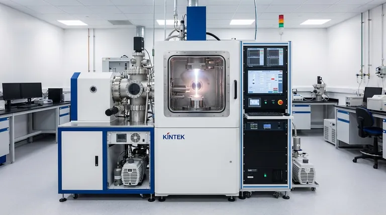
Electron beam evaporation is a cornerstone technology for creating high-performance thin films across a vast range of industries, from aerospace and electronics to advanced optics and manufacturing. Its primary applications involve depositing dense, pure coatings that provide exceptional resistance to heat, wear, and chemicals, or that impart specific optical and electrical properties to a surface.
The true value of electron beam evaporation lies in its ability to efficiently vaporize materials with very high melting points. This unique capability makes it the preferred method for creating durable protective coatings and complex optical layers that would be difficult or impossible to achieve with other techniques.
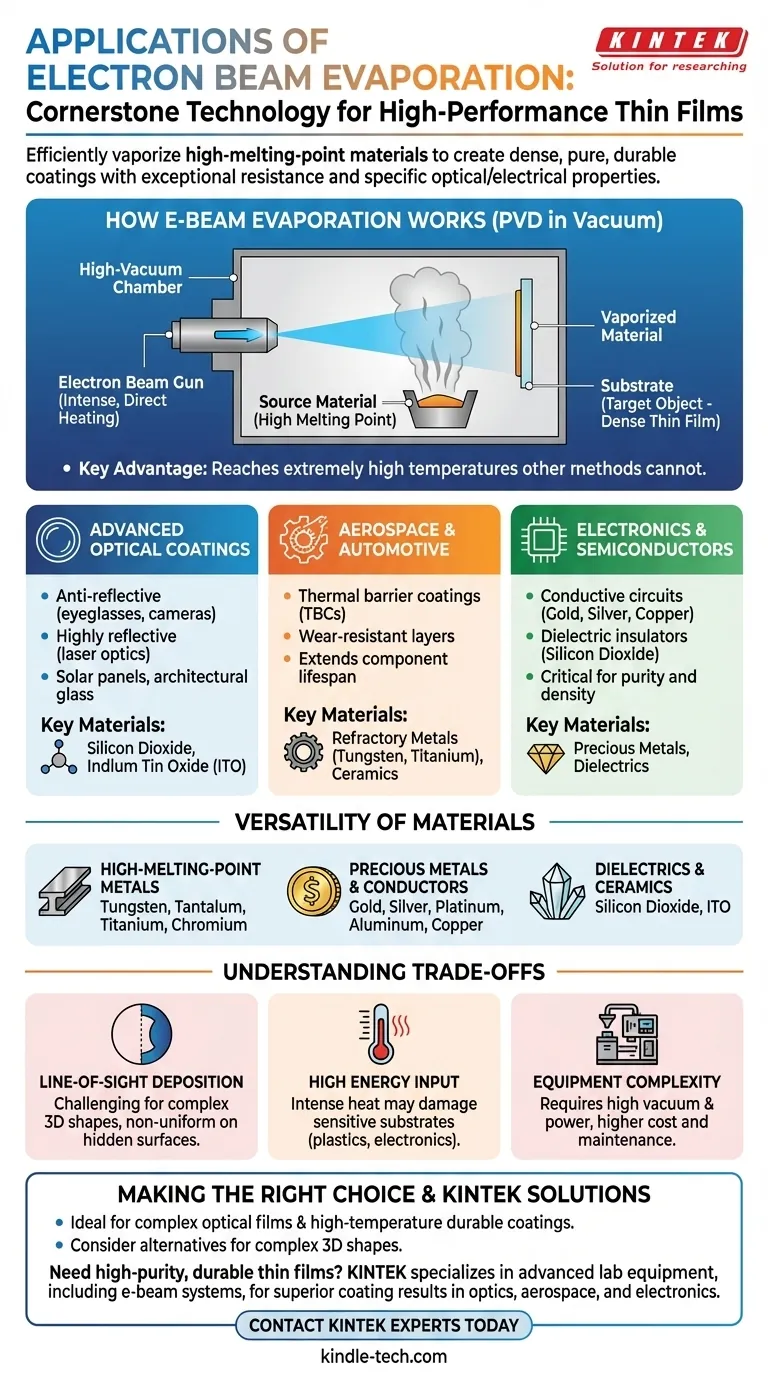
How E-Beam Evaporation Works
The Core Process: PVD in a Vacuum
Electron beam (e-beam) evaporation is a type of physical vapor deposition (PVD). The entire process takes place inside a high-vacuum chamber to ensure the final coating is extremely pure.
A high-power beam of electrons is fired at a source material, such as a block of ceramic or metal. This intense energy heats the material until it evaporates into a vapor. This vapor then travels through the vacuum and condenses on the target object, or substrate, forming a dense, thin film.
The Key Advantage: Intense, Direct Heating
The electron beam transfers heat directly and efficiently to the source material. This allows the process to reach extremely high temperatures that other methods cannot.
This is the central reason for its versatility—it can vaporize materials with very high melting points, from refractory metals to durable ceramics.
Key Application Areas by Industry
Advanced Optical Coatings
This is one of the most prominent applications of e-beam evaporation. The process provides the high degree of control needed to create precise layers that manipulate light.
Examples include anti-reflective coatings for eyeglasses and camera lenses, highly reflective coatings for laser optics, and specific films used in solar panels and architectural glass.
Aerospace and Automotive
In these industries, components are often exposed to extreme heat and friction. E-beam evaporation is used to apply thermal barrier coatings (TBCs) and wear-resistant coatings.
These durable ceramic or metallic layers protect critical engine parts and other components, extending their lifespan and improving performance and safety.
Electronics and Semiconductors
The purity and density of e-beam deposited films are critical for manufacturing electronic components.
It is used to lay down thin films of conductive metals like gold, silver, and copper for circuits, as well as dielectric materials like silicon dioxide for insulators.
The Versatility of Materials
The ability to handle high-temperature materials is what truly sets e-beam evaporation apart. It can deposit a uniquely broad range of materials.
High-Melting-Point Metals
This includes refractory metals known for their hardness and heat resistance, such as tungsten, tantalum, titanium, and chromium.
Precious Metals and Conductors
The process is also highly effective for depositing precious and conductive metals, including gold, silver, platinum, aluminum, and copper.
Dielectrics and Ceramics
E-beam evaporation is ideal for applying ceramic and dielectric compounds with high melting points, such as silicon dioxide and indium tin oxide (ITO), which are crucial for optical and electronic applications.
Understanding the Trade-offs
Line-of-Sight Deposition
A key limitation of e-beam evaporation is that it is a line-of-sight process. The vapor travels in a straight line from the source to the substrate.
This can make it challenging to coat complex, three-dimensional shapes with uniform thickness, as surfaces not directly facing the source will receive little to no coating.
High Energy Input
The intense energy from the electron beam can cause significant heating of the substrate. This can be a problem for heat-sensitive materials like plastics or certain electronic components, potentially causing damage.
Equipment Complexity
E-beam systems are complex and require high-vacuum environments and high-voltage power supplies. This makes the initial investment and ongoing maintenance more demanding compared to some other coating technologies.
Making the Right Choice for Your Goal
- If your primary focus is creating complex, multi-layer optical films: Electron beam evaporation offers the precision and material flexibility required for superior performance.
- If your primary focus is depositing durable, heat-resistant coatings from refractory metals or ceramics: This method is one of the most effective and efficient options available.
- If your primary focus is coating complex 3D shapes uniformly: You may need to explore alternative PVD processes like sputtering that do not have the same line-of-sight limitations.
Ultimately, understanding these core capabilities allows you to leverage e-beam evaporation for creating coatings that define the performance of modern technology.
Summary Table:
| Application Area | Key Materials Used | Primary Benefits |
|---|---|---|
| Optical Coatings | Silicon Dioxide, Indium Tin Oxide (ITO) | Anti-reflective, highly reflective layers for lenses and lasers |
| Aerospace & Automotive | Ceramics, Refractory Metals (Tungsten, Titanium) | Thermal barrier coatings (TBCs), wear resistance |
| Electronics & Semiconductors | Gold, Silver, Copper, Silicon Dioxide | Conductive circuits, dielectric insulators |
| General High-Performance Coatings | Precious Metals (Gold, Platinum), Aluminum | Chemical resistance, specific electrical properties |
Need a high-purity, durable thin film for your project?
KINTEK specializes in advanced lab equipment, including electron beam evaporation systems, to help you achieve superior coating results. Whether you're developing cutting-edge optics, protecting aerospace components, or manufacturing sensitive electronics, our expertise ensures you get the precise material deposition you need.
Contact our experts today to discuss how our solutions can enhance your product's performance and reliability!
Visual Guide
Related Products
- Electron Beam Evaporation Coating Tungsten Crucible and Molybdenum Crucible for High Temperature Applications
- Electron Beam Evaporation Coating Oxygen-Free Copper Crucible and Evaporation Boat
- Electron Beam Evaporation Coating Gold Plating Tungsten Molybdenum Crucible for Evaporation
- Electron Beam Evaporation Coating Conductive Boron Nitride Crucible BN Crucible
- E Beam Crucibles Electron Gun Beam Crucible for Evaporation
People Also Ask
- What is e-beam evaporation used for? Precision Coating for Optics, Aerospace & Electronics
- What is the temperature of e-beam evaporation? Mastering the Two-Zone Thermal Process for Precision Films
- What is the deposition rate of e-beam evaporation? Control Thin Film Quality and Speed
- What are the applications of e-beam evaporation? Achieve High-Purity Coatings for Optics & Electronics
- What materials are used in electron beam evaporation? Master High-Purity Thin Film Deposition


