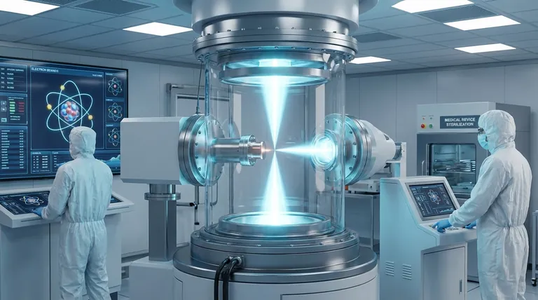
At its core, an electron beam is a highly versatile and controllable energy source. This stream of accelerated electrons is used across a vast range of industries for applications including high-resolution imaging at the atomic level, precise welding and manufacturing of critical components, large-scale medical device sterilization, and fundamental scientific research.
The unparalleled utility of electron beams comes from two fundamental properties: their negative charge and their tiny mass. These characteristics allow them to be precisely steered and focused by magnetic and electric fields, delivering highly concentrated energy or acting as a subatomic probe with a wavelength far shorter than visible light.
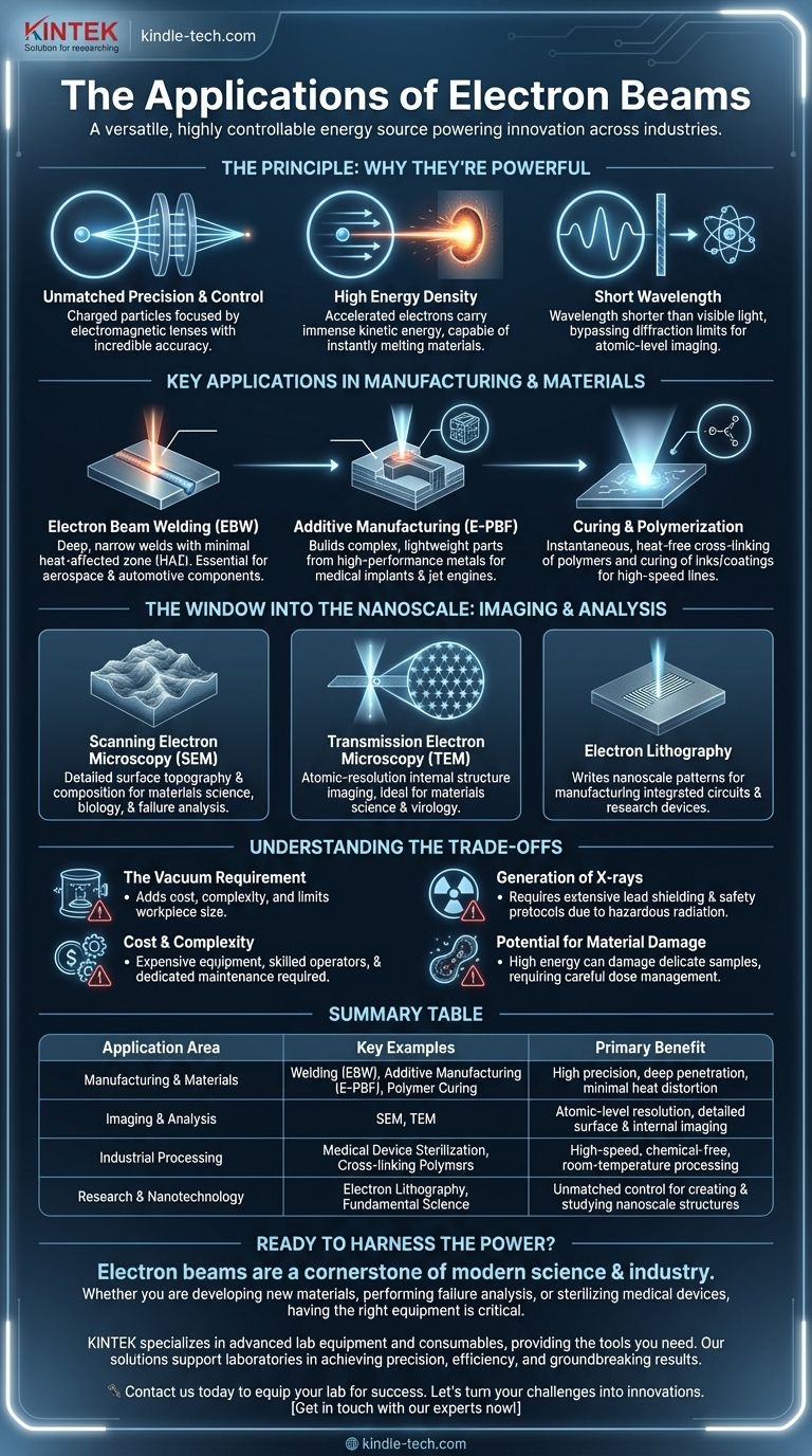
The Principle: Why Electron Beams Are So Powerful
To understand the applications, you must first grasp the core principles that make electron beams so effective. Their behavior is governed by a few key physical properties.
### Unmatched Precision and Control
Because electrons are charged particles, their path can be deflected and focused with incredible accuracy using electromagnetic lenses.
This is analogous to how glass lenses focus light, but with far greater control. It allows an electron beam to be aimed at a spot millions of times smaller than the tip of a needle.
### High Energy Density
By accelerating electrons to high speeds (a significant fraction of the speed of light), they carry substantial kinetic energy.
When this beam is focused onto a tiny area, the energy density—the amount of energy per unit area—becomes immense. This allows the beam to instantly melt or even vaporize any known material.
### Short Wavelength for High Resolution
In quantum mechanics, all moving particles, including electrons, have a corresponding wavelength. The faster an electron moves, the shorter its wavelength.
This extremely short wavelength allows electron beams to bypass the diffraction limit that restricts conventional light microscopes, enabling them to image individual atoms.
Key Applications in Manufacturing and Materials Processing
In industrial settings, the electron beam is a workhorse, valued for its power and precision. The entire process must occur in a vacuum to prevent the electrons from scattering off air molecules.
### Electron Beam Welding (EBW)
EBW uses a highly focused beam to melt and fuse metals. Its key advantage is producing extremely deep, narrow, and clean welds with a very small heat-affected zone (HAZ).
This minimizes distortion and maintains the strength of the surrounding material, making it essential for aerospace, automotive, and power generation components.
### Additive Manufacturing (E-PBF)
In Electron Beam Powder Bed Fusion (E-PBF), the beam selectively melts layers of fine metal powder to build complex, three-dimensional parts.
This technology excels at creating strong, lightweight components from high-performance materials like titanium and nickel-based superalloys, often for medical implants and jet engine parts.
### Curing and Polymerization
A less intense, broad electron beam can be used to initiate chemical reactions. It is widely used to cross-link polymers or cure inks and coatings.
This process is nearly instantaneous and generates very little heat, making it ideal for treating heat-sensitive materials or for high-speed production lines.
The Window into the Nanoscale: Imaging and Analysis
The wave-like nature of electrons makes them the ultimate tool for exploring the world beyond the limits of light.
### Scanning Electron Microscopy (SEM)
In an SEM, the beam is scanned across a sample's surface. Detectors capture the secondary electrons knocked loose from the surface, creating a detailed image of the sample's topography and composition.
This provides a rich, 3D-like view of surfaces, used for failure analysis, materials science, and biology.
### Transmission Electron Microscopy (TEM)
A TEM passes a broad beam of high-energy electrons through an ultra-thin sample. The resulting image reveals the material's internal structure, crystal lattice, and even individual atoms.
It is the definitive tool for atomic-resolution imaging in materials science, virology, and nanotechnology.
### Electron Lithography
Borrowing from microscopy, electron lithography uses a finely focused beam to "write" patterns onto a sensitive surface layer called a resist.
This technique is fundamental to manufacturing prototype integrated circuits and creating nanoscale devices for research.
Understanding the Trade-offs
Despite their power, electron beams are not a universal solution. Their application comes with significant constraints and challenges that must be considered.
### The Vacuum Requirement
Nearly all electron beam applications require a high-vacuum environment. Creating and maintaining this vacuum adds significant cost, complexity, and limits the size of the workpiece.
### Generation of X-rays
When high-energy electrons strike a material, they decelerate rapidly and produce X-rays (Bremsstrahlung radiation). This is a serious safety hazard that requires extensive lead shielding and rigorous safety protocols, adding to facility costs.
### Cost and Complexity
Electron beam systems—from the electron gun to the vacuum pumps and high-voltage power supplies—are complex and expensive pieces of equipment. They require skilled operators and dedicated maintenance.
### Potential for Material Damage
The same high energy that makes electron beams useful for imaging and processing can also damage delicate samples. For biological specimens or certain polymers, the electron dose must be carefully managed to avoid destroying the very structure being observed.
Making the Right Choice for Your Goal
Selecting the right technology depends entirely on your specific objective. Electron beams offer a range of solutions tailored to different needs.
- If your primary focus is high-integrity manufacturing: Consider Electron Beam Welding for its deep penetration and minimal material distortion, especially with reactive or high-temperature metals.
- If your primary focus is atomic-scale internal imaging: Transmission Electron Microscopy is the definitive tool for resolving the internal crystal structure or organization of a material.
- If your primary focus is surface analysis and topography: Scanning Electron Microscopy provides unparalleled depth of field and detailed images of a sample's surface features.
- If your primary focus is industrial-scale sterilization: Electron beam processing offers a fast, room-temperature method for sterilizing heat-sensitive medical devices without chemical residues.
By understanding these core principles and trade-offs, you can effectively determine where electron beam technology can solve challenges that are impossible with conventional tools.
Summary Table:
| Application Area | Key Examples | Primary Benefit |
|---|---|---|
| Manufacturing & Materials | Welding (EBW), Additive Manufacturing (E-PBF), Polymer Curing | High precision, deep penetration, minimal heat distortion |
| Imaging & Analysis | Scanning Electron Microscopy (SEM), Transmission Electron Microscopy (TEM) | Atomic-level resolution, detailed surface and internal imaging |
| Industrial Processing | Medical Device Sterilization, Cross-linking Polymers | High-speed, chemical-free, room-temperature processing |
| Research & Nanotechnology | Electron Lithography, Fundamental Science | Unmatched control for creating and studying nanoscale structures |
Ready to harness the power of electron beam technology in your lab?
Electron beams are a cornerstone of modern science and industry, enabling breakthroughs from atomic imaging to high-integrity manufacturing. Whether you are developing new materials, performing failure analysis, or sterilizing medical devices, having the right equipment is critical.
KINTEK specializes in advanced lab equipment and consumables, providing the tools you need to leverage technologies like electron beams. Our solutions support laboratories in achieving precision, efficiency, and groundbreaking results.
Contact us today to discuss how we can equip your lab for success. Let’s turn your challenges into innovations.
Get in touch with our experts now!
Visual Guide
Related Products
- Electron Beam Evaporation Coating Oxygen-Free Copper Crucible and Evaporation Boat
- Electron Beam Evaporation Coating Tungsten Crucible and Molybdenum Crucible for High Temperature Applications
- E Beam Crucibles Electron Gun Beam Crucible for Evaporation
- Electron Beam Evaporation Coating Conductive Boron Nitride Crucible BN Crucible
- Electron Beam Evaporation Coating Gold Plating Tungsten Molybdenum Crucible for Evaporation
People Also Ask
- What is the voltage of e-beam evaporation? Achieve Precise Thin-Film Deposition
- What is the deposition rate of e-beam evaporation? Control Thin Film Quality and Speed
- How is an electron beam evaporator cooled during deposition? Essential Thermal Management for Stable Processes
- What is e-beam evaporation used for? Precision Coating for Optics, Aerospace & Electronics
- What is the current of e-beam evaporation? A Guide to High-Purity Thin Film Deposition


