Plasma-Enhanced Chemical Vapor Deposition (PECVD) is a critical semiconductor process used to deposit thin, high-quality films onto a substrate. Unlike traditional methods that rely solely on high heat, PECVD uses an energized plasma to initiate a chemical reaction between reactant gases, allowing the deposition to occur at much lower temperatures, typically around 350°C.
The central advantage of PECVD is its ability to bypass the need for high temperatures. By using plasma to drive the chemical reaction, it enables the creation of high-performance films on thermally sensitive materials without causing damage, stress, or unwanted diffusion between layers.
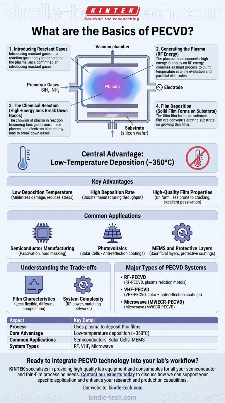
How PECVD Works: The Core Mechanism
PECVD is a carefully controlled process that transforms gases into a solid film inside a vacuum chamber. The entire mechanism can be understood in four distinct stages.
Introducing Reactant Gases
The process begins by introducing specific precursor gases into a reaction chamber. For example, to create a silicon nitride film, gases like silane (SiH₄) and ammonia (NH₃) are used.
Generating the Plasma
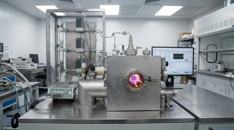
An electric field, typically radio frequency (RF), is applied between two parallel electrodes within the chamber. This energy ionizes the gas molecules, stripping electrons and creating a highly reactive state of matter known as a plasma, often visible as a characteristic glow discharge.
The Chemical Reaction
This energetic plasma is the key to the process. The highly reactive ions and radicals within the plasma break down the stable precursor gases, inducing a chemical reaction that would otherwise require extreme heat.
Film Deposition
The products of this chemical reaction then deposit onto the surface of the substrate (such as a silicon wafer), building up a thin, solid, and uniform film. For solar cells, this might be a silicon nitride (SiNx) layer that acts as an anti-reflection coating.
Key Advantages of the PECVD Process
The use of plasma provides several distinct advantages over purely thermal deposition methods, making it indispensable in modern manufacturing.
Low Deposition Temperature
This is the most significant benefit. By operating at lower temperatures, PECVD minimizes thermal damage to the substrate and any existing layers. It also reduces internal stress caused by mismatches in thermal expansion between the film and the substrate.
High Deposition Rate
PECVD can achieve relatively high deposition rates, which is highly beneficial for manufacturing throughput. This is especially true for producing amorphous and microcrystalline films efficiently.
High-Quality Film Properties
The process creates highly uniform layers that are less prone to cracking compared to some conventional CVD methods. These films serve critical functions, such as providing electrical passivation and optical anti-reflection.
Common Applications Across Industries
PECVD is not a niche technology; it is a workhorse in several high-tech fields for creating functional layers.
Semiconductor Manufacturing
It is widely used to create passivation layers that protect device surfaces, hard masking for patterning, and dielectric films for insulation.
Photovoltaics (Solar Cells)
In solar cell production, PECVD is essential for depositing silicon nitride anti-reflection coatings. This layer both reduces light reflection and passivates the silicon surface, significantly improving the cell's conversion efficiency.
MEMS and Protective Layers
The technology is also used to build sacrificial layers in Micro-Electro-Mechanical Systems (MEMS) and to apply hard, protective coatings on various materials.
Understanding the Trade-offs
While powerful, PECVD is not a universal solution. It's essential to understand its specific characteristics to make informed engineering decisions.
Film Characteristics
The resulting films from PECVD can be less flexible than those produced by other methods, such as Low-Pressure Chemical Vapor Deposition (LPCVD). The composition and density can differ from high-temperature processes.
System Complexity
The inclusion of plasma generation equipment (RF power sources, matching networks) adds complexity to the system compared to a purely thermal CVD reactor.
Major Types of PECVD Systems
Over time, several variations of PECVD have been developed to optimize the process for specific outcomes and materials.
Radio Frequency (RF-PECVD)
This is the most common type, using a radio frequency electric field to create the plasma. It can be further divided into capacitive coupling (CCP) and inductive coupling (ICP) methods.
Very High Frequency (VHF-PECVD)
Using a higher frequency (VHF) can lower the electron temperature while increasing plasma density. This often results in higher deposition rates and can improve film quality.
Microwave (MWECR-PECVD)
This advanced method uses microwave energy and magnetic fields to achieve electron cyclotron resonance (ECR). This creates a very high-density plasma, allowing for the formation of extremely high-quality films at very low temperatures.
Making the Right Choice for Your Goal
Selecting a deposition technology depends entirely on the priorities of your application.
- If your primary focus is protecting a temperature-sensitive substrate: PECVD is the definitive choice due to its low-temperature operation, which prevents thermal damage.
- If your primary focus is manufacturing throughput for amorphous films: PECVD offers a significant advantage with its characteristically high deposition rates.
- If your primary focus is achieving specific film properties like high purity or flexibility: You may need to evaluate alternatives like LPCVD, which can offer different material characteristics due to its thermal-only process.
By understanding these core principles, you can effectively leverage PECVD's unique capabilities for advanced material fabrication and device engineering.
Summary Table:
| Aspect | Key Detail |
|---|---|
| Process | Uses plasma to deposit thin films from gases onto a substrate. |
| Core Advantage | Low-temperature deposition (~350°C), protecting sensitive materials. |
| Common Applications | Semiconductor passivation, solar cell anti-reflection coatings, MEMS. |
| System Types | RF-PECVD, VHF-PECVD, Microwave PECVD (MWECR-PECVD). |
Ready to integrate PECVD technology into your lab's workflow?
KINTEK specializes in providing high-quality lab equipment and consumables for all your semiconductor and thin-film processing needs. Whether you are developing advanced solar cells, MEMS devices, or semiconductor components, our expertise ensures you get the right PECVD solution for high-performance, low-temperature deposition.
Contact our experts today to discuss how we can support your specific application and enhance your research and production capabilities.
Visual Guide
Related Products
- RF PECVD System Radio Frequency Plasma-Enhanced Chemical Vapor Deposition RF PECVD
- Chemical Vapor Deposition CVD Equipment System Chamber Slide PECVD Tube Furnace with Liquid Gasifier PECVD Machine
- Inclined Rotary Plasma Enhanced Chemical Vapor Deposition PECVD Equipment Tube Furnace Machine
- Inclined Rotary Plasma Enhanced Chemical Vapor Deposition PECVD Equipment Tube Furnace Machine
- 915MHz MPCVD Diamond Machine Microwave Plasma Chemical Vapor Deposition System Reactor
People Also Ask
- What is plasma enhanced chemical Vapour deposition process used for fabrication of? A Guide to Low-Temperature Thin Films
- What is plasma enhanced chemical vapour deposition PECVD used for? Enable Low-Temp Thin Films for Electronics & Solar
- What is an example of PECVD? RF-PECVD for High-Quality Thin Film Deposition
- Why is a Matching Network Indispensable in RF-PECVD for Siloxane Films? Ensure Stable Plasma and Uniform Deposition
- What is plasma CVD? Unlock Low-Temperature Thin Film Deposition for Sensitive Materials


