Knowledge What are the basics of thin films? Master the Technology Behind Modern Electronics and Coatings
Author avatar

Tech Team · Kintek Solution

Updated 2 weeks ago

What are the basics of thin films? Master the Technology Behind Modern Electronics and Coatings

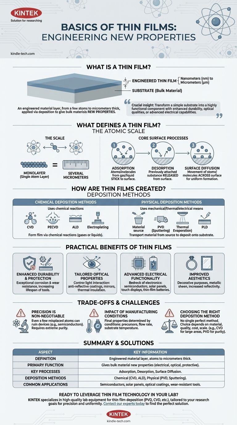
At its core, a thin film is an engineered layer of material ranging from just a few atoms to several micrometers in thickness. These films are applied to a surface, or substrate, through a process called deposition. This controlled synthesis is not merely a coating but a fundamental step in creating countless modern products, from semiconductor chips to advanced optics.

The crucial insight is that thin films are designed to give a bulk material entirely new properties. By precisely controlling material layers at an atomic or molecular scale, we can transform a simple substrate into a highly functional component with enhanced durability, specific optical qualities, or advanced electrical capabilities.

What Defines a Thin Film?

A thin film's behavior is dictated by its incredibly small scale and the physics that dominate at the atomic level. Understanding these principles is key to understanding their function.

The Scale: Nanometers to Micrometers

A thin film's thickness can be as small as a single layer of atoms (monolayer) or extend up to several micrometers. This precise control over thickness is what enables their specialized properties.

The Core Processes at the Surface

Three phenomena govern how a thin film forms and interacts with its environment:

  • Adsorption: The process where atoms or molecules from a gas or liquid stick to the substrate's surface.
  • Desorption: The opposite of adsorption, where a previously attached substance is released from the surface.
  • Surface Diffusion: The movement of atoms and molecules across the surface, which is critical for forming a uniform, high-quality film.

How Are Thin Films Created? The Deposition Process

Creating a thin film involves depositing material onto a substrate using highly controlled methods. These techniques are broadly divided into two families: chemical and physical.

Chemical Deposition Methods

These methods use chemical reactions to form the film on the substrate. The precursors are often gases or liquids.

Common examples include Chemical Vapor Deposition (CVD), Plasma-Enhanced CVD (PECVD), Atomic Layer Deposition (ALD), and electroplating.

Physical Deposition Methods

These techniques use mechanical, thermal, or electrical means to transport material from a source and deposit it onto the substrate's surface.

This category includes Physical Vapor Deposition (PVD) methods like sputtering and thermal evaporation, as well as Pulsed Laser Deposition (PLD).

The Practical Benefits of Thin Films

Applying a thin film fundamentally alters the surface of a material, providing a wide range of functional and aesthetic advantages.

Enhanced Durability and Protection

One of the most common uses is to protect the underlying substrate. Thin films provide exceptional corrosion and wear resistance, significantly increasing the lifespan and durability of tools and components.

Tailored Optical Properties

Multiple layers of thin films can be engineered to control how light interacts with a surface. This is the principle behind anti-reflective coatings on eyeglasses, mirrors on reflector lamps, and thermal insulation on architectural glass.

Advanced Electrical Functionality

Thin films are the bedrock of modern electronics. They are used to create semiconductors, thin-film photovoltaic cells (solar panels), touch-panel displays, and even next-generation thin-film batteries.

Improved Aesthetics

Beyond function, thin films are used for decorative purposes. They can enhance a substrate's appearance with a metallic sheen, as seen on jewelry or bathroom fittings, or make it more reflective.

Understanding the Trade-offs and Challenges

While the benefits are significant, the process of creating high-quality thin films is demanding and fraught with challenges. The choice of method involves critical trade-offs.

Precision is Non-Negotiable

The quality of the thin film is paramount. In applications like semiconductors, even a few misplaced atoms can render the entire device useless. This requires manufacturing environments with extreme purity and control.

The Impact of Manufacturing Conditions

The final properties of the film are determined by the specific conditions during deposition. Factors like the type of precursor chemicals, their flow rate onto the surface, and the substrate temperature must be precisely managed to achieve the desired outcome.

Choosing the Right Deposition Method

No single deposition method is perfect for all applications. Chemical methods like CVD can provide excellent uniformity over large areas, while physical methods like PVD are valued for their purity. The choice depends on the material, desired quality, cost, and scale of production.

Making the Right Choice for Your Goal

Selecting the appropriate thin film strategy depends entirely on the intended application and performance requirements.

  • If your primary focus is high-performance electronics: You need atomic-level precision, making methods like Atomic Layer Deposition (ALD) or Molecular Beam Epitaxy (MBE) critical.
  • If your primary focus is protecting a large surface from corrosion: Cost-effective and scalable methods like electroplating or certain types of sputtering are often the best choice.
  • If your primary focus is creating specialized optical coatings: Deposition techniques that offer precise control over layer thickness, such as various forms of CVD or PVD, are essential.

Understanding these fundamentals allows you to see thin films not just as coatings, but as a foundational technology for manipulating the properties of matter.

Summary Table:

Aspect Key Information
Definition Engineered material layer, from atoms to micrometers thick, applied to a substrate.
Primary Function Gives a bulk material new properties (electrical, optical, protective).
Key Processes Adsorption, Desorption, Surface Diffusion.
Deposition Methods Chemical (CVD, ALD) and Physical (PVD, Sputtering).
Common Applications Semiconductors, solar panels, anti-reflective coatings, wear-resistant tools.

Ready to leverage thin film technology in your lab?

Whether you are developing next-generation electronics, creating specialized optical coatings, or need to enhance the durability of your components, choosing the right deposition equipment is critical. KINTEK specializes in high-quality lab equipment for thin film deposition, including systems for PVD, CVD, and more.

We provide solutions tailored to your specific research and production goals, helping you achieve the precision, uniformity, and performance your projects demand.

Contact our experts today to discuss your application and find the perfect thin film solution for your laboratory.

Related Products

People Also Ask

Related Products

Chemical Vapor Deposition CVD Equipment System Chamber Slide PECVD Tube Furnace with Liquid Gasifier PECVD Machine

Chemical Vapor Deposition CVD Equipment System Chamber Slide PECVD Tube Furnace with Liquid Gasifier PECVD Machine

KT-PE12 Slide PECVD System: Wide power range, programmable temp control, fast heating/cooling with sliding system, MFC mass flow control & vacuum pump.

RF PECVD System Radio Frequency Plasma-Enhanced Chemical Vapor Deposition RF PECVD

RF PECVD System Radio Frequency Plasma-Enhanced Chemical Vapor Deposition RF PECVD

RF-PECVD is an acronym for "Radio Frequency Plasma-Enhanced Chemical Vapor Deposition." It deposits DLC (Diamond-like carbon film) on germanium and silicon substrates. It is utilized in the 3-12um infrared wavelength range.

Customer Made Versatile CVD Tube Furnace Chemical Vapor Deposition Chamber System Equipment

Customer Made Versatile CVD Tube Furnace Chemical Vapor Deposition Chamber System Equipment

Get your exclusive CVD furnace with KT-CTF16 Customer Made Versatile Furnace. Customizable sliding, rotating, and tilting functions for precise reactions. Order now!

Split Chamber CVD Tube Furnace with Vacuum Station Chemical Vapor Deposition System Equipment Machine

Split Chamber CVD Tube Furnace with Vacuum Station Chemical Vapor Deposition System Equipment Machine

Efficient split chamber CVD furnace with vacuum station for intuitive sample checking and quick cooling. Up to 1200℃ max temperature with accurate MFC mass flowmeter control.

1200℃ Split Tube Furnace with Quartz Tube Laboratory Tubular Furnace

1200℃ Split Tube Furnace with Quartz Tube Laboratory Tubular Furnace

KT-TF12 split tube furnace: high-purity insulation, embedded heating wire coils, and max. 1200C. Widely used for new materials and chemical vapour deposition.

Multi Zone Laboratory Quartz Tube Furnace Tubular Furnace

Multi Zone Laboratory Quartz Tube Furnace Tubular Furnace

Experience precise, efficient thermal testing with our Multi Zone Tube Furnace. Independent heating zones and temperature sensors allow for controlled high-temperature gradient heating fields. Order now for advanced thermal analysis!

Rotary Tube Furnace Split Multi Heating Zone Rotating Tube Furnace

Rotary Tube Furnace Split Multi Heating Zone Rotating Tube Furnace

Multi zone rotary furnace for high-precision temperature control with 2-8 independent heating zones. Ideal for lithium ion battery electrode materials and high-temperature reactions. Can work under vacuum and controlled atmosphere.

Spark Plasma Sintering Furnace SPS Furnace

Spark Plasma Sintering Furnace SPS Furnace

Discover the benefits of Spark Plasma Sintering Furnaces for rapid, low-temperature material preparation. Uniform heating, low cost & eco-friendly.

Vacuum Induction Melting Spinning System Arc Melting Furnace

Vacuum Induction Melting Spinning System Arc Melting Furnace

Develop metastable materials with ease using our Vacuum Melt Spinning System. Ideal for research and experimental work with amorphous and microcrystalline materials. Order now for effective results.

High Temperature Muffle Oven Furnace for Laboratory Debinding and Pre Sintering

High Temperature Muffle Oven Furnace for Laboratory Debinding and Pre Sintering

KT-MD High temperature debinding and pre-sintering furnace for ceramic materials with various molding processes. Ideal for electronic components such as MLCC and NFC.

1400℃ Laboratory Quartz Tube Furnace with Alumina Tube Tubular Furnace

1400℃ Laboratory Quartz Tube Furnace with Alumina Tube Tubular Furnace

Looking for a tube furnace for high-temperature applications? Our 1400℃ Tube Furnace with Alumina Tube is perfect for research and industrial use.

Vacuum Heat Treat Sintering Brazing Furnace

Vacuum Heat Treat Sintering Brazing Furnace

A vacuum brazing furnace is a type of industrial furnace used for brazing, a metalworking process that joins two pieces of metal using a filler metal that melts at a lower temperature than the base metals. Vacuum brazing furnaces are typically used for high-quality applications where a strong, clean joint is required.

Laboratory Muffle Oven Furnace Bottom Lifting Muffle Furnace

Laboratory Muffle Oven Furnace Bottom Lifting Muffle Furnace

Efficiently produce batches with excellent temperature uniformity using our Bottom Lifting Furnace. Features two electric lifting stages and advanced temperature control up to 1600℃.

Vertical Laboratory Quartz Tube Furnace Tubular Furnace

Vertical Laboratory Quartz Tube Furnace Tubular Furnace

Elevate your experiments with our Vertical Tube Furnace. Versatile design allows for operation under various environments and heat treatment applications. Order now for precise results!

1700℃ Laboratory Quartz Tube Furnace with Alumina Tube Tubular Furnace

1700℃ Laboratory Quartz Tube Furnace with Alumina Tube Tubular Furnace

Looking for a high-temperature tube furnace? Check out our 1700℃ Tube Furnace with Alumina Tube. Perfect for research and industrial applications up to 1700C.

1800℃ Muffle Oven Furnace for Laboratory

1800℃ Muffle Oven Furnace for Laboratory

KT-18 muffle furnace with Japan Al2O3 polycrystalline fibe and Silicon Molybdenum heating element, up to 1900℃, PID temperature control and 7" smart touch screen. Compact design, low heat loss, and high energy efficiency. Safety interlock system and versatile functions.

1400℃ Controlled Atmosphere Furnace with Nitrogen and Inert Atmosphere

1400℃ Controlled Atmosphere Furnace with Nitrogen and Inert Atmosphere

Achieve precise heat treatment with KT-14A controlled atmosphere furnace. Vacuum sealed with a smart controller, it's ideal for lab and industrial use up to 1400℃.

1700℃ Controlled Atmosphere Furnace Nitrogen Inert Atmosphere Furnace

1700℃ Controlled Atmosphere Furnace Nitrogen Inert Atmosphere Furnace

KT-17A Controlled atmosphere furnace: 1700℃ heating, vacuum sealing technology, PID temperature control, and versatile TFT smart touch screen controller for laboratory and industrial use.

Controlled Nitrogen Inert Hydrogen Atmosphere Furnace

Controlled Nitrogen Inert Hydrogen Atmosphere Furnace

KT-AH Hydrogen atmosphere furnace - induction gas furnace for sintering/annealing with built-in safety features, dual housing design, and energy-saving efficiency. Ideal for lab and industrial use.

Vacuum Heat Treat and Molybdenum Wire Sintering Furnace for Vacuum Sintering

Vacuum Heat Treat and Molybdenum Wire Sintering Furnace for Vacuum Sintering

A vacuum molybdenum wire sintering furnace is a vertical or bedroom structure, which is suitable for withdrawal, brazing, sintering and degassing of metal materials under high vacuum and high temperature conditions. It is also suitable for dehydroxylation treatment of quartz materials.


Leave Your Message